Thin-film transistor, and preparation method, array substrate and display thereof

A technology of thin film transistors and array substrates, applied in the display field, can solve the problems of increasing leakage current, affecting the display quality of the display, affecting the working characteristics of the TFT, etc.

Active Publication Date: 2014-01-08
BOE TECH GRP CO LTD +1
View PDF7 Cites 36 Cited by
  • Summary
  • Abstract
  • Description
  • Claims
  • Application Information

AI Technical Summary

Problems solved by technology

[0003] However, since the carrier mobility of the zinc oxide oxynitride (ZnON) active layer is more than 200 times that of the traditional amorphous silicon active layer, excessive carrier mobility will lead to leakage current of the TFT increase, affect the working characteristics of TFT, reduce the reliability of the TFT array substrate, and thus affect the display quality of the display

Method used


Image

  • Thin-film transistor, and preparation method, array substrate and display thereof
  • Thin-film transistor, and preparation method, array substrate and display thereof
  • Thin-film transistor, and preparation method, array substrate and display thereof

Examples


Embodiment 1

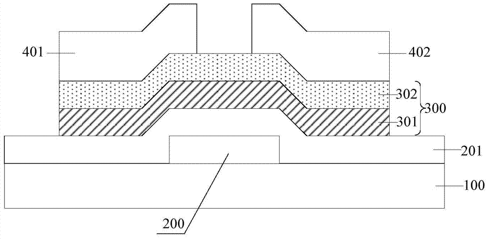
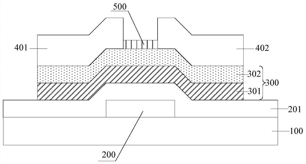
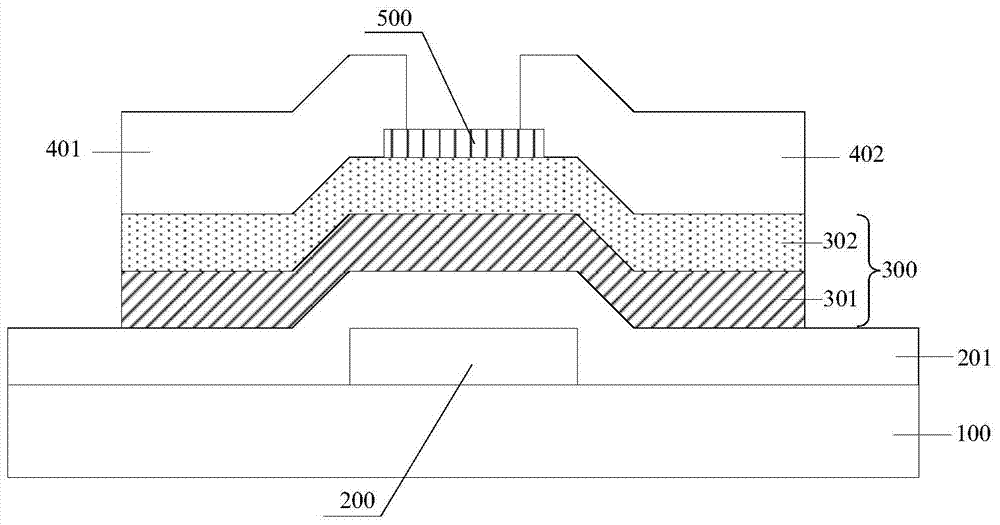
[0057] Embodiment 1. Embodiment 1 of the present invention provides a bottom-gate thin film transistor. Refer to figure 2 As shown, it includes: a gate 200, a gate insulating layer 201, an active layer 300, a source 401 and a drain 402; wherein, the active layer 300 includes a layer of zinc oxide semiconductor first active layer 301 and A second active layer 302 of gallium and aluminum co-doped zinc oxynitride semiconductor, and the first active layer 301 is arranged on the gate insulating layer 201, and the second active layer 302 is arranged on above the first active layer 301; the thin film transistor further includes an etch barrier layer 500, and the etch barrier layer 500 is disposed on the gap corresponding to the gap between the source electrode 401 and the drain electrode 402. above the second active layer 302 .

[0058] Wherein, the thickness of the first active layer 301 of a layer of zinc oxynitride semiconductor is 1.5 times the thickness of the second active la...

Embodiment 2

[0061] Embodiment 2. Embodiment 2 of the present invention provides a top-gate thin film transistor. Refer to Figure 4 As shown, it includes: a source electrode 401 and a drain electrode 402, an active layer 300, a gate insulating layer 201, and a gate electrode 200 sequentially arranged on a substrate 100; wherein, the active layer 300 includes a layer of zinc oxynitride semiconductor A first active layer 301 and a second active layer 302 of germanium-doped zinc oxynitride semiconductor, and the second active layer 302 is arranged on the source 401 and the drain 402, the first An active layer 301 is disposed on the second active layer 302 .

[0062] Wherein, the thickness of the first active layer 301 of a layer of zinc oxynitride semiconductor is the same as the thickness of the second active layer 302 of a layer of germanium-doped zinc oxynitride semiconductor; and, the germanium-doped The total concentration is 2.0%.

[0063] Since the material of the second active laye...


PUM


Abstract

The embodiment of the invention provides a thin-film transistor, and a preparation method, an array substrate and a display thereof, relating to the field of displaying technology and capable of reducing the current leakage and ensuring the performance reliability of the thin-film transistor while maintaining the high on-state current of the thin-film transistor. The thin-film transistor comprises a grid electrode, a grid insulating layer, an active layer, a source electrode and a drain electrode, wherein the active layer comprises a first active layer and a second active layer, the first active layer is arranged at one side close to the grid insulating layer, the second active layer is arranged at one side close to the source electrode and the drain electrode; the charge carrier mobility of the first active layer is higher than that of the second active layer. The invention provides the production method of the thin-film transistor capable of reducing the current leakage of the thin-film transistor while needing to maintain the high on-state current of the thin-film transistor, and a production method of the array substrate and the display of the thin-film transistor.

Description

technical field [0001] The invention relates to the field of display technology, in particular to a thin film transistor and a preparation method thereof, an array substrate and a display. Background technique [0002] At present, as the size of the display continues to increase, the frequency of the driving circuit continues to increase, and a thin film transistor with higher carrier mobility is required as a switch of the pixel unit in the display. The traditional thin film transistor (TFT) uses amorphous silicon material as the active layer, and its carrier mobility is only 0.5cm 2 / V·s, for a large-scale display with a size of more than 80 inches, its driving frequency reaches 120Hz, correspondingly, the active layer of the thin film transistor needs to have a thickness of 1.0cm 2 / V·s above carrier mobility, obviously, the carrier mobility of amorphous silicon TFT is difficult to meet the driving needs of large-size displays. Therefore, people turn their research atte...

Claims


Application Information

Patent Timeline
Patent Type & Authority Applications(China)
IPC IPC(8): H01L29/786H01L29/24H01L27/12H01L21/34
CPCH01L29/7869H01L21/02521H01L21/02554H01L21/0257H01L27/12H01L27/1225H01L29/24H01L29/66742H01L29/66969H01L29/786H01L29/78696H01L29/0607H01L29/22
Inventor 黄常刚张振宇
Owner BOE TECH GRP CO LTD
Why Eureka
Try Eureka