Warp correction device and warp correction method for semiconductor element substrate
A technology of semiconductors and components, applied in the field of bending correction equipment, can solve problems such as unsuitability for mass production, high yield, and increased load in the grinding process
- Summary
- Abstract
- Description
- Claims
- Application Information
AI Technical Summary
Problems solved by technology
Method used
Image


Examples
Embodiment Construction
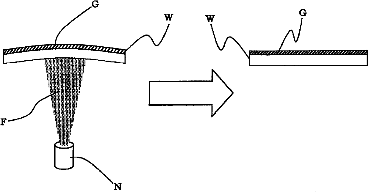
[0040] The bending correction device according to the embodiment will be described with reference to the drawings. The curvature correcting device is, for example, a device that corrects curvature by injecting a spray material onto a substrate for a semiconductor element.
[0041] The substrate for semiconductor elements whose curvature is corrected by the curvature correction device is, for example, a substrate composed of sapphire, SiC, GaAs, GaP, GaAlAs, etc., and is used to form a semiconductor film, such as a GaN series compound semiconductor film, on the main surface to form a light-emitting substrate. Substrates for semiconductor elements such as diode (LED) elements and laser diode (LD) elements.
[0042] figure 1 It is a schematic diagram showing a method of correcting warping of a substrate for a semiconductor element by blasting. The substrate W for a semiconductor element such as a sapphire wafer on which a semiconductor film G of a GaN-based compound or the like...
PUM
 Abstract
Description
Claims
Application Information