Self-aligned multi-patterning mask layer and formation method thereof

A technology of multiple patterning and mask layers, applied in the field of semiconductor manufacturing, can solve problems such as affecting the electrical performance of semiconductor devices

Inactive Publication Date: 2014-01-15
SEMICON MFG INT (SHANGHAI) CORP
View PDF4 Cites 32 Cited by
  • Summary
  • Abstract
  • Description
  • Claims
  • Application Information

AI Technical Summary

Problems solved by technology

[0008] But after using the above-mentioned self-aligned double pattern as a mask to etch the material layer 20 to be etched, the side walls of the material layer 20 to

Method used


Image

  • Self-aligned multi-patterning mask layer and formation method thereof
  • Self-aligned multi-patterning mask layer and formation method thereof
  • Self-aligned multi-patterning mask layer and formation method thereof

Examples


Embodiment Construction

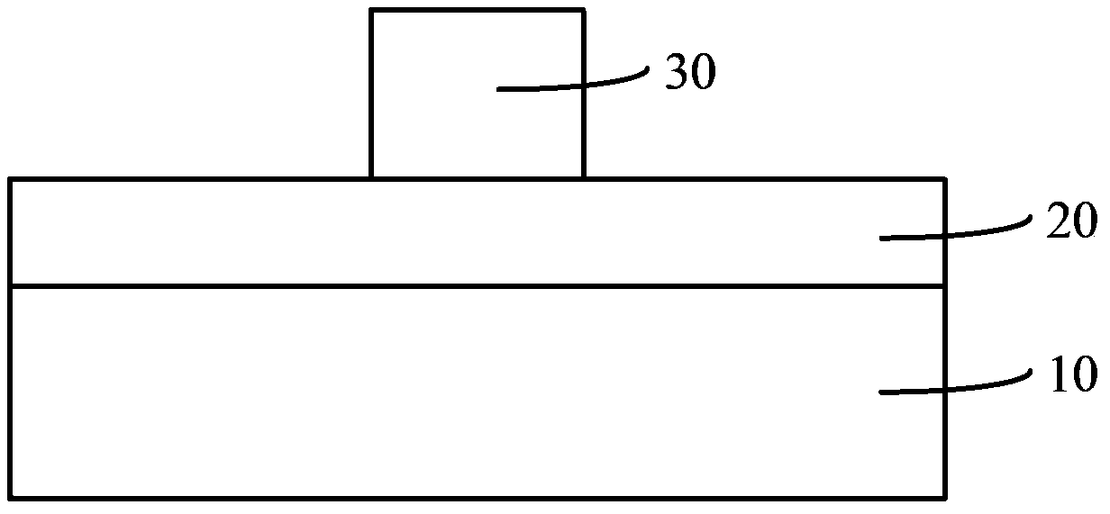
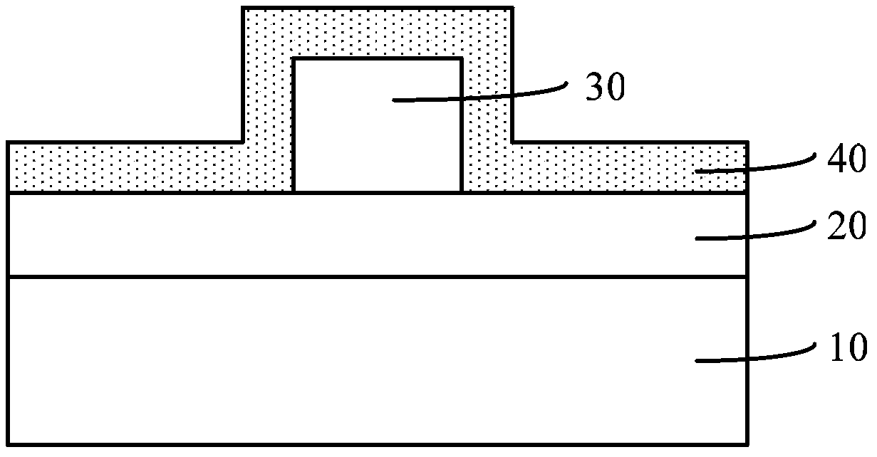
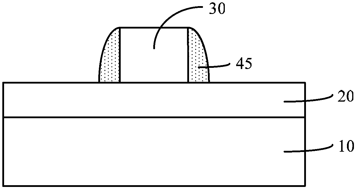
[0039] In the background art, it is known that after the material layer to be etched is etched using the self-aligned dual pattern of the prior art as a mask, the sidewalls of the material layer to be etched corresponding to both sides of the sidewall have different morphologies, which will affect The electrical properties of subsequent semiconductor devices. The inventor found through research that the different morphologies of the sidewalls of the material layer to be etched are mainly caused by the different cross-sectional shapes of the sidewalls on both sides of the sidewalls. The sidewalls of the sidewalls close to the sacrificial layer and the semiconductor The surface of the substrate is vertical, but because the sidewall is formed by maskless etching of the hard mask material layer, the sidewall shape of the sidewall on the side away from the sacrificial layer is curved. The surface of the etched material layer is far away from the surface of the material layer to be e...


PUM


Abstract

The invention relates to a self-aligned multi-patterning mask layer and a formation method thereof. The formation method comprises the following steps that: a semiconductor substrate is provided and a to-be-etched material layer is formed at the surface of the semiconductor substrate; a sacrificial material layer is formed at the surface of the to-be-etched material layer; etching is carried out on the sacrificial material layer to form a sacrificial layer, wherein the dimension of the portion, approaching the to-be-etched material layer, of the sacrificial layer is smaller than that of the portion, far away from the to-be-etched material layer, of the sacrificial layer; and a side wall is formed at the surface of the side wall of the sacrificial layer, wherein the portions of the two sides of the side wall are inclined towards the middle portion of the side wall from a position at the surface of the to-be-etched material layer to a position far away from the surface of the to-be-etched material layer. Because the portions of the two sides of the side wall are inclined towards the middle portion of the side wall and the profile shapes of the portions of the two sides of the side wall are identical with each other, the shapes of side walls of the to-be-etched material layer formed by etching by using the side wall as the mask subsequently are identical, so that the electrical performance of the semiconductor device that is formed subsequently is not influenced.

Description

Technical field [0001] The present invention relates to the field of semiconductor manufacturing, in particular to a self-aligned multiple patterned mask layer and a forming method thereof. Background technique [0002] In the field of semiconductor manufacturing, photoresist materials are used to transfer a mask image to one or more layers of materials, for example, to transfer the mask image to a metal layer, a dielectric layer, or a semiconductor substrate. However, as the feature size of the semiconductor process continues to shrink, it becomes more and more difficult to form a mask pattern with a small feature size in the material layer using a photolithography process. [0003] In order to improve the integration of semiconductor devices, the industry has proposed a variety of dual patterning processes, among which a self-aligned double patterning (SADP) process is one of them. The US patent document with the publication number US2009 / 0146322A1 discloses a method for etching...

Claims


Application Information

Patent Timeline
IPC IPC(8): H01L21/027G03F7/00
CPCH01L21/027G03F7/70466H01L21/28008
Inventor 吴汉明洪中山
Owner SEMICON MFG INT (SHANGHAI) CORP
Why Eureka
Try Eureka