Infrared sensor manufacturing method of Zigbee
A technology of an infrared sensor and a manufacturing method, which is applied in the field of sensors, can solve the problems of large heat capacity of the device, cumbersome processes, rate limitation, etc., and achieves the effects of fast response speed, simple process and high reliability
- Summary
- Abstract
- Description
- Claims
- Application Information
AI Technical Summary
Problems solved by technology
Method used
Image

Examples
Embodiment 1
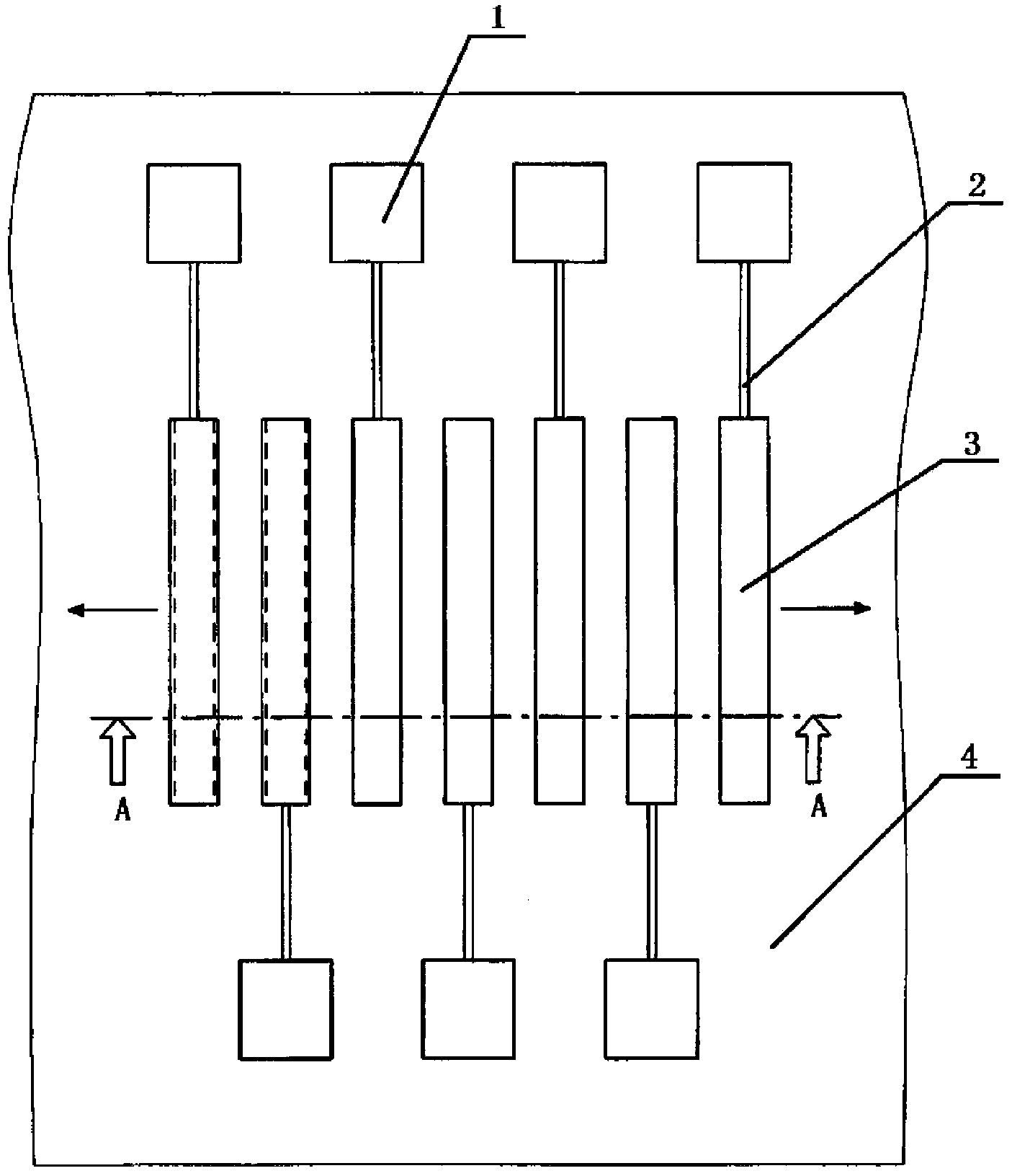
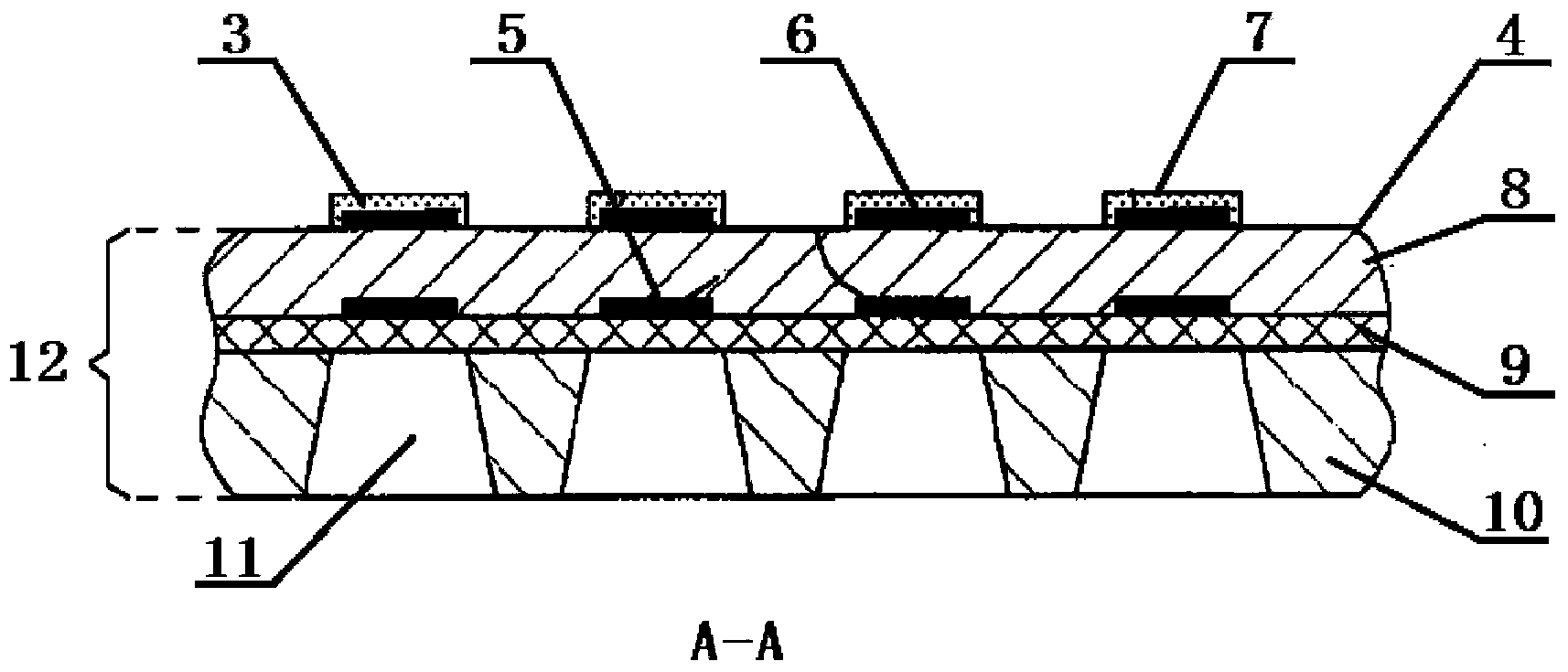
[0028] like figure 1 and 2 As shown, a Zigbee infrared sensor manufacturing method is carried out according to the following steps:
[0029] (1) Provide a substrate 10, which is an SOI substrate;
[0030] (2) A plurality of grooves 11 are finely processed in the substrate 10, filled with the first release sacrificial layer in the grooves 11, and covered with a diaphragm 9 on the surface of the substrate 10, and the diaphragm 9 is porous polyimide;
[0031] (3) Forming the lower electrode 5 on the diaphragm 9;
[0032] (4) performing a gas phase release process to remove the first release sacrificial layer;
[0033] (5) Forming a pyroelectric layer 8 on the diaphragm 9 and the lower electrode 5;
[0034] (6) Form an infrared structural absorption layer 3 on the upper surface of the substrate 12, and locally form a plurality of pixels 7 in the substrate 12. In the formation step of the infrared structural absorption layer 3, deposit a colloidal particle dispersion, thereby ...
Embodiment 2
[0042] like figure 1 and 2 As shown, a Zigbee infrared sensor manufacturing method is carried out according to the following steps:
[0043] (1) Provide a substrate 10, which is an SOI substrate;
[0044] (2) A plurality of grooves 11 are finely processed in the substrate 10, filled with the first release sacrificial layer in the grooves 11, and covered with a diaphragm 9 on the surface of the substrate 10, and the diaphragm 9 is porous polyimide;
[0045] (3) Forming the lower electrode 5 on the diaphragm 9;
[0046] (4) performing a gas phase release process to remove the first release sacrificial layer;
[0047] (5) Forming a pyroelectric layer 8 on the diaphragm 9 and the lower electrode 5;
[0048] (6) Form an infrared structural absorption layer 3 on the upper surface of the substrate 12, and locally form a plurality of pixels 7 in the substrate 12. In the formation step of the infrared structural absorption layer 3, deposit a colloidal particle dispersion, thereby ...
PUM
 Abstract
Description
Claims
Application Information
 - R&D Engineer
- R&D Manager
- IP Professional
- Industry Leading Data Capabilities
- Powerful AI technology
- Patent DNA Extraction
Browse by: Latest US Patents, China's latest patents, Technical Efficacy Thesaurus, Application Domain, Technology Topic.
© 2024 PatSnap. All rights reserved.Legal|Privacy policy|Modern Slavery Act Transparency Statement|Sitemap