Semiconductor chip packaging structure and packaging method

A technology of chip packaging structure and packaging method, which is applied in the direction of semiconductor devices, semiconductor/solid-state device manufacturing, semiconductor/solid-state device components, etc., can solve the problem of reducing thickness, etc., and achieve thickness reduction, convenient quantitative production and use, and fast processing Effect

Inactive Publication Date: 2014-01-22
桂林微网半导体有限责任公司
View PDF10 Cites 5 Cited by
  • Summary
  • Abstract
  • Description
  • Claims
  • Application Information

AI Technical Summary

Problems solved by technology

Therefore, it is difficult to significantly reduce the thickness of the existing chip packaging structure, and the total thickness of

Method used


Image

  • Semiconductor chip packaging structure and packaging method
  • Semiconductor chip packaging structure and packaging method
  • Semiconductor chip packaging structure and packaging method

Examples


Embodiment Construction

[0037] Embodiment of semiconductor chip packaging structure

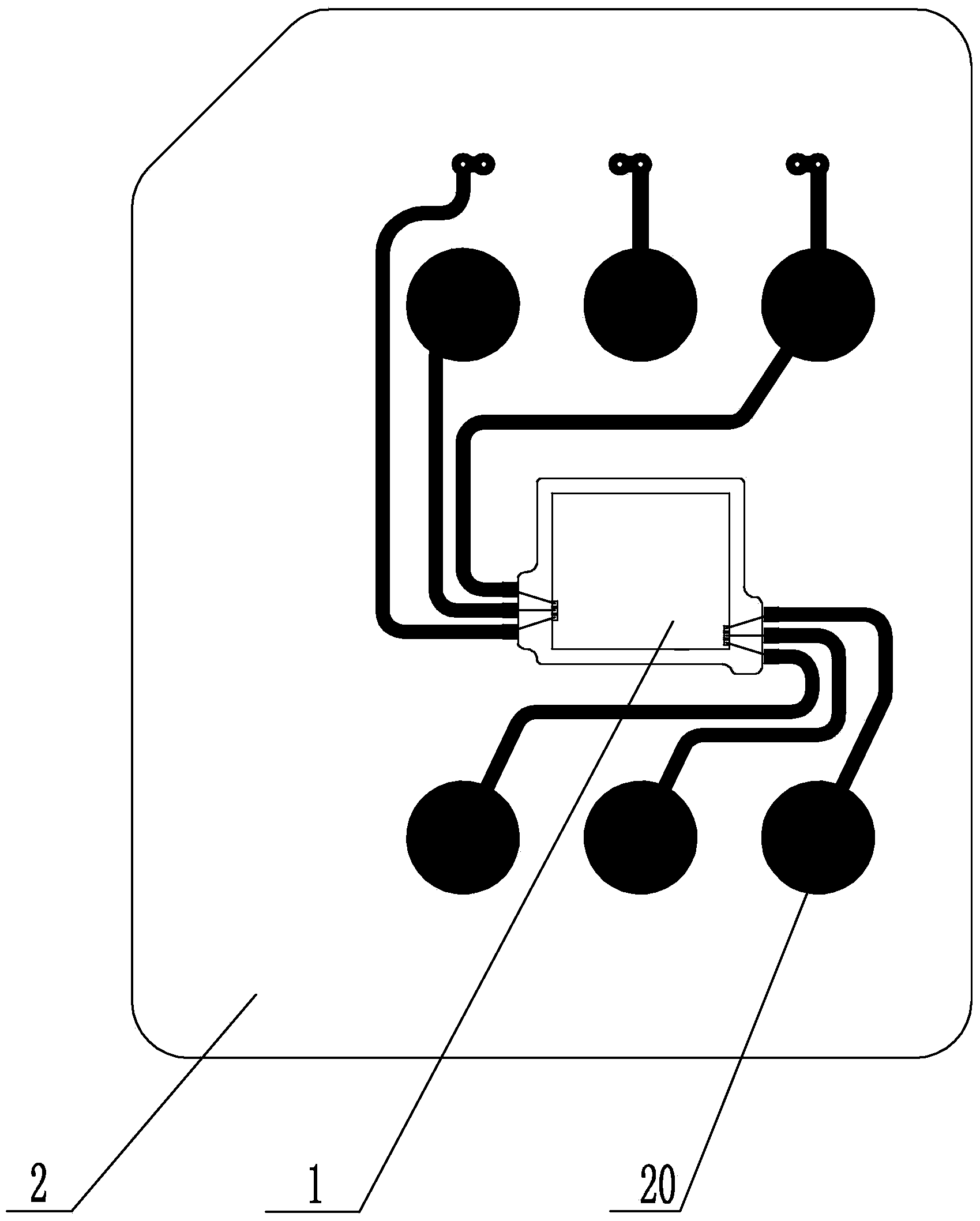
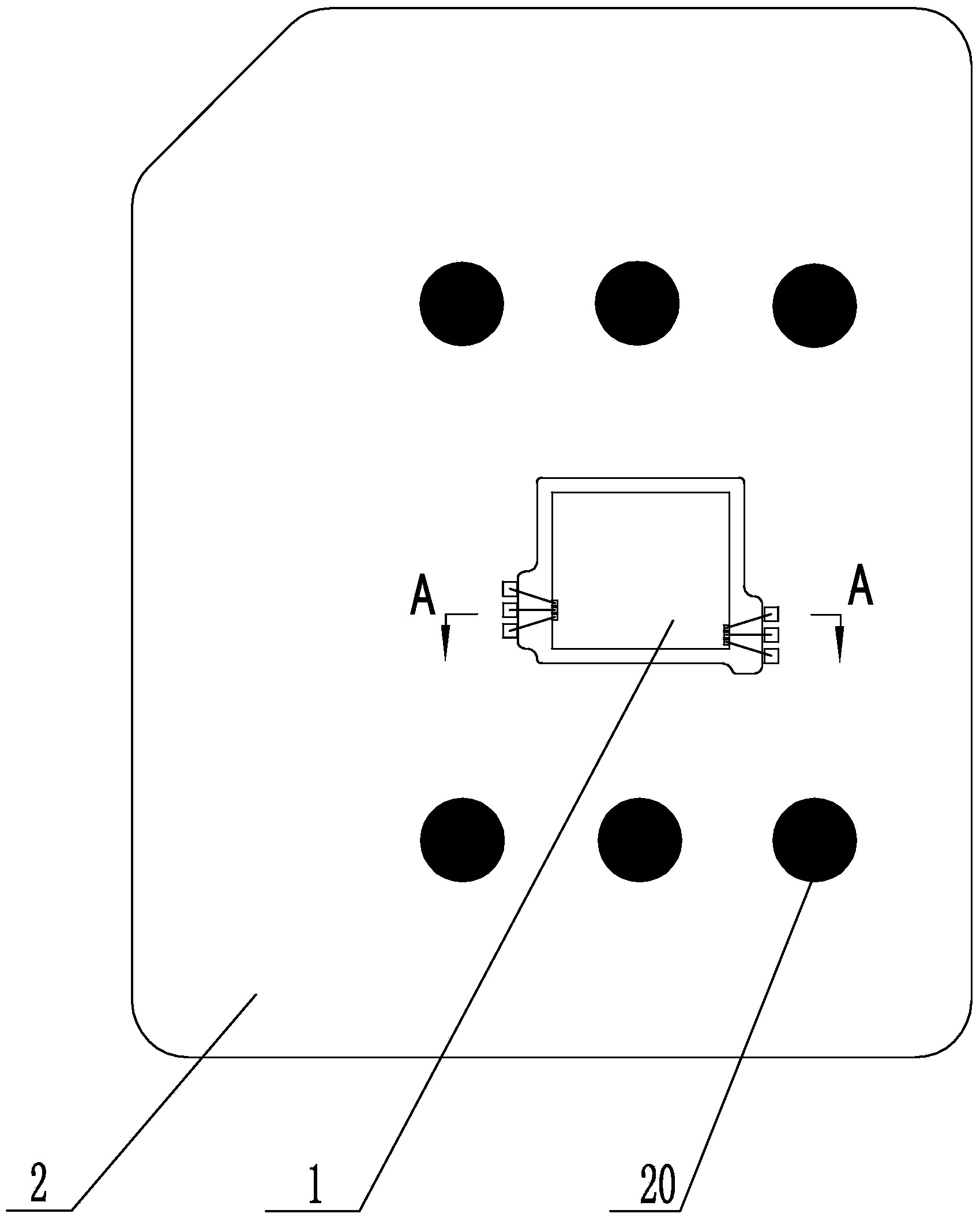
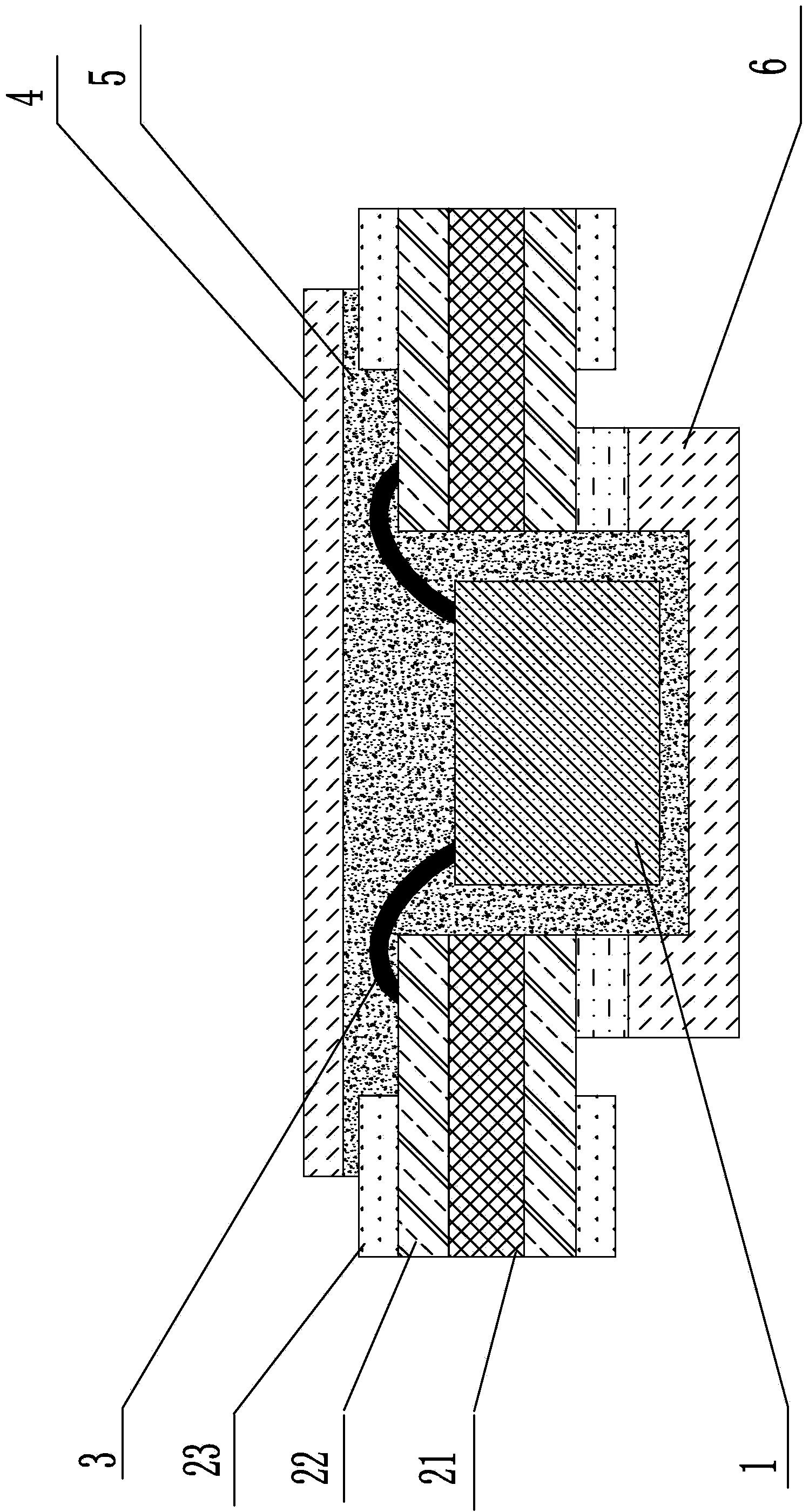
[0038] The embodiment of this chip packaging structure is a patch card (or a film card) for a SIM card of a mobile phone, such as Figures 1 to 3 shown. The upper and lower surfaces of the substrate 21 of the circuit board 2 are covered with a conductive layer 22, and the conductive layer 22 on the circuit board forms pins, contacts 20 and conductive lines, and the corresponding contacts 20 and pins are connected through conductive lines, such as figure 1 As shown, it is covered with a solder resist layer 23, and the solder resist layer 23 has corresponding holes at the pins and contacts, so that the pins and contacts are exposed, as figure 2 shown.

[0039] In this example, the chip 1 is rectangular, and the rectangular through-holes on the circuit board 2 that cooperate with the chip 1 are mounting holes, whose length and width are 0.1 mm larger than the length and width of the chip 1 . The circuit board in th...


PUM


Abstract

The invention discloses a semiconductor chip packaging structure and a packaging method. A through hole matched with a chip in a circuit board is a mounting hole; a lower protective layer seals the bottom of the mounting hole, and is fixedly connected with the circuit board; the lower protective layer in the mounting hole is a chip loading platform; the chip is wholly or partially embedded into the mounting hole; the surface of the chip is flush with or lower than the upper surface of the circuit board; the bottom surface of the chip is bonded with the chip loading platform; leads are connected with connection points of the chip and pins of the circuit board; and solid sealing glue is filled between a hole wall of the mounting hole of the circuit board and the chip, and coats and seals the upper surface of the chip and the leads. The packaging method comprises the steps that the through hole of the circuit board is processed; the lower protective layer seals the through hole of the circuit board; the surface of the lower protective layer is smooth, or a raised groove matched with the chip is formed in the surface of the lower protective layer; the bottom surface of the chip is bonded with the chip loading platform; the connection points of the chip are linked with the leads of the pins of the circuit board; and the solid sealing glue fills and coats the chip and the leads. According to the packaging structure and the packaging method, the thickness of the circuit board is utilized effectively; the thickness of the packaging structure is reduced significantly; the solid sealing glue protects the leads and the connection points; and a product is stable and reliable.

Description

technical field [0001] The invention relates to the technical field of chip packaging, in particular to a semiconductor chip packaging structure and packaging method. Background technique [0002] The packaging shell of the semiconductor integrated circuit chip plays the role of placing, fixing, sealing, protecting the chip and enhancing the electrothermal performance. The contacts of the chip are connected to the pins protruding from the packaging shell with wires. The other device establishes the connection. Packaging has become a necessary process for the production of CPU and other LSI integrated circuit chips. [0003] Because the development trend of various electronic products is light, thin and compact, it is required that the semiconductor chip package should be as thin and small as possible. There are a variety of semiconductor chip packaging structures that use a structure in which the chip is placed on the circuit board (that is, COB Chip On Board). This struct...

Claims


Application Information

Patent Timeline
IPC IPC(8): H01L23/31H01L23/498H01L21/56H01L21/60
CPCH01L2224/48091H01L2224/73265H01L2224/92247H01L2924/00014
Inventor 黄一平宾志滔莫华邦
Owner 桂林微网半导体有限责任公司
Why Eureka
Try Eureka