Gallium nitride light emitting diode and preparation method thereof

A technology of light-emitting diodes and gallium nitride, applied in semiconductor/solid-state device manufacturing, electrical components, circuits, etc., can solve the problem of affecting the three-dimensional growth time of high-temperature buffer layers, it is difficult to control the surface morphology of GaN epitaxy, and it is difficult to obtain high-quality GaN epitaxy and other issues, to achieve the effect of prolonging the growth time in three-dimensional space, reducing the epitaxial dislocation density, and reducing the lattice mismatch

Active Publication Date: 2014-01-22
HC SEMITEK CORP
View PDF3 Cites 16 Cited by
  • Summary
  • Abstract
  • Description
  • Claims
  • Application Information

AI Technical Summary

Problems solved by technology

[0004] In the process of realizing the present invention, the inventors found that there are at least the following problems in the prior art: after the low-temperature buffer layer is grown, the temperature is raised directly to grow the high-temperature buffer layer, which makes it easier to form two-dimensional growth, resulting in a large gap between the islands in the island structure. It is easy to connect, which affects the three-dimensional growth time of the high-temperature buffer layer. In this way, it is difficult to obtain high-quality GaN epitaxy, and it is difficult to control the surface morphology of GaN epitaxy

Method used


Image

  • Gallium nitride light emitting diode and preparation method thereof
  • Gallium nitride light emitting diode and preparation method thereof
  • Gallium nitride light emitting diode and preparation method thereof

Examples


Embodiment Construction

[0030] In order to make the object, technical solution and advantages of the present invention clearer, the implementation manner of the present invention will be further described in detail below in conjunction with the accompanying drawings.

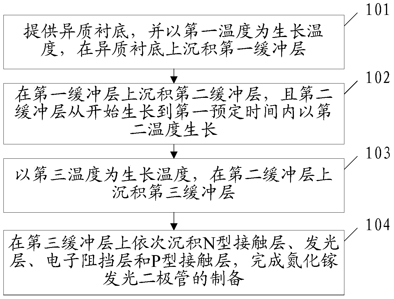
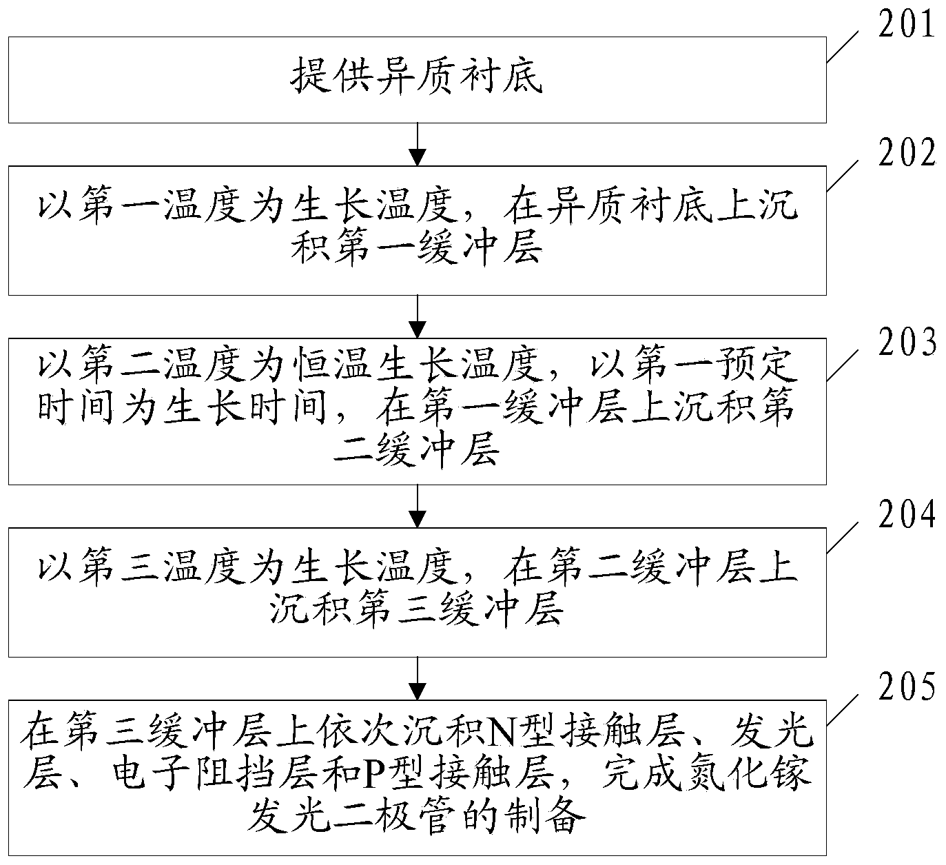
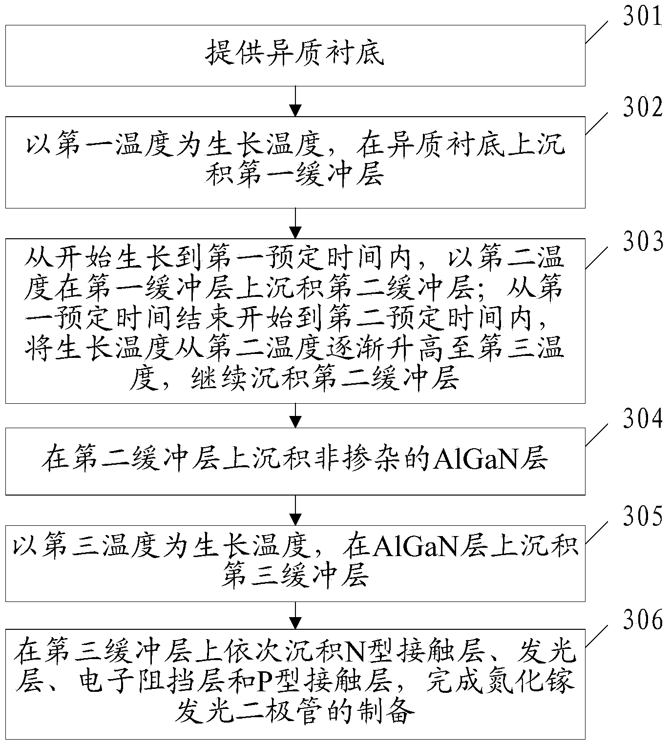
[0031] figure 1 A method for preparing a gallium nitride light-emitting diode provided by an embodiment of the present invention is shown. see figure 1 , the method includes:

[0032] Step 101: providing a foreign substrate, and depositing a first buffer layer on the foreign substrate with the first temperature as the growth temperature.

[0033] Alternatively, the first temperature may be 520°C.

[0034] Step 102: Deposit a second buffer layer on the first buffer layer, and grow the second buffer layer at a second temperature within a first predetermined time from the start of growth.

[0035] Wherein, the first temperature


PUM


Abstract

The invention discloses a gallium nitride light emitting diode and a preparation method thereof and belongs to the field of light emitting diodes. The method comprises the following steps: providing a foreign substrate, and depositing a first buffering layer on the foreign substrate by taking a first temperature as a growing temperature; depositing a second buffering layer on the first buffering layer and enabling the second buffering layer to grow at a second temperature from the time of beginning to grow to a first pre-set time, wherein the first temperature is lower than the second temperature and the differential value range of the first temperature and the second temperature is 410-460 DEG C; depositing a third buffering layer on the second buffering layer by taking a third temperature as the growing temperature, wherein the second temperature is lower than the third temperature; and sequentially depositing an N type contact layer, a light-emitting layer, an electronic barrier layer and a P type contact layer on the third buffering layer to finish the preparation of the gallium nitride light emitting diode. The light emitting diode is prepared by adopting the method. The growing starting temperature of the second buffering layer is between the growing temperature of the first buffering layer and the growing temperature of the third buffering layer and the second buffering layer has the buffering and protection effects on the third buffering layer.

Description

technical field [0001] The invention relates to the field of light-emitting diodes (Light-Emitting Diode, LED for short), in particular to a gallium nitride light-emitting diode and a preparation method thereof. Background technique [0002] A gallium nitride (GaN) LED includes a substrate and an epitaxy consisting mainly of GaN grown on the substrate. Based on the principle that the crystal lattice of the substrate and epitaxy needs to match, for GaN epitaxy, the ideal substrate is a single crystal of III-nitride. However, the single crystal area developed at this stage is small and the price is high, so heterogeneous substrates (such as sapphire substrates) are commonly used to grow GaN epitaxy. [0003] There is inevitably a lattice mismatch between the heterogeneous substrate and GaN epitaxy. In order to slow down the lattice mismatch between the heterogeneous substrate and GaN epitaxy, a buffer layer is usually grown on the substrate first, and then GaN epitaxy is gro...

Claims


Application Information

Patent Timeline
Patent Type & Authority Applications(China)
IPC IPC(8): H01L33/12H01L33/00
CPCH01L21/02458H01L33/0075
Inventor 胡清富魏世祯
Owner HC SEMITEK CORP
Why Eureka
Try Eureka