High-voltage NLDMOS (N-type laterally diffused metal oxide semiconductor) structure for electrostatic protection

An electrostatic protection, high voltage technology, applied in the direction of circuits, electrical components, semiconductor devices, etc., can solve the problems of unfavorable anti-latch effect and low opening current, so as to achieve the effect of not affecting the electrostatic protection ability and improving the anti-latch ability

Active Publication Date: 2014-01-29
SHANGHAI HUAHONG GRACE SEMICON MFG CORP
View PDF2 Cites 8 Cited by
  • Summary
  • Abstract
  • Description
  • Claims
  • Application Information

AI Technical Summary

Problems solved by technology

but, figure 2 The low turn-on current of the structure is detrimental to the anti-latch-up effect

Method used


Image

  • High-voltage NLDMOS (N-type laterally diffused metal oxide semiconductor) structure for electrostatic protection
  • High-voltage NLDMOS (N-type laterally diffused metal oxide semiconductor) structure for electrostatic protection
  • High-voltage NLDMOS (N-type laterally diffused metal oxide semiconductor) structure for electrostatic protection

Examples


Embodiment Construction

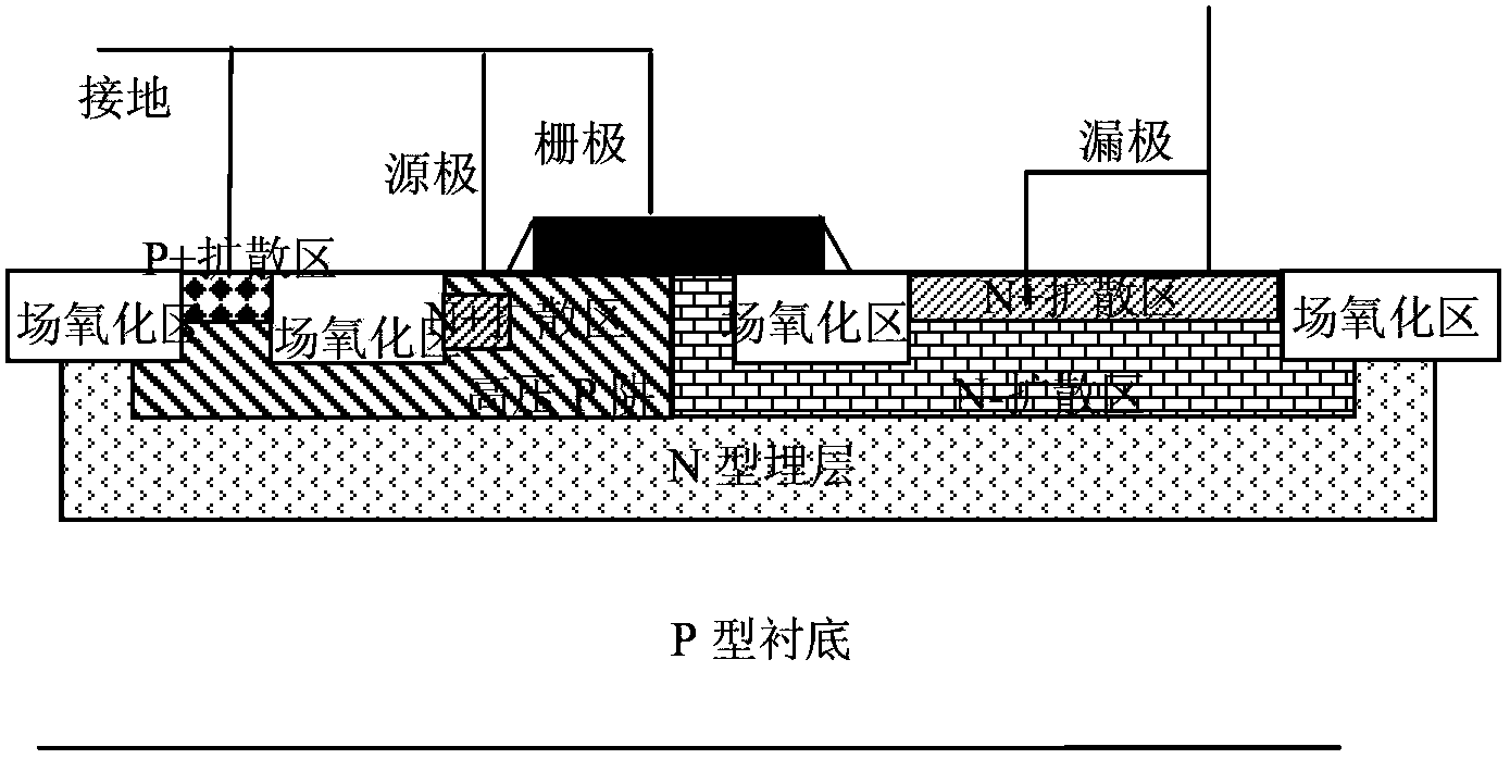
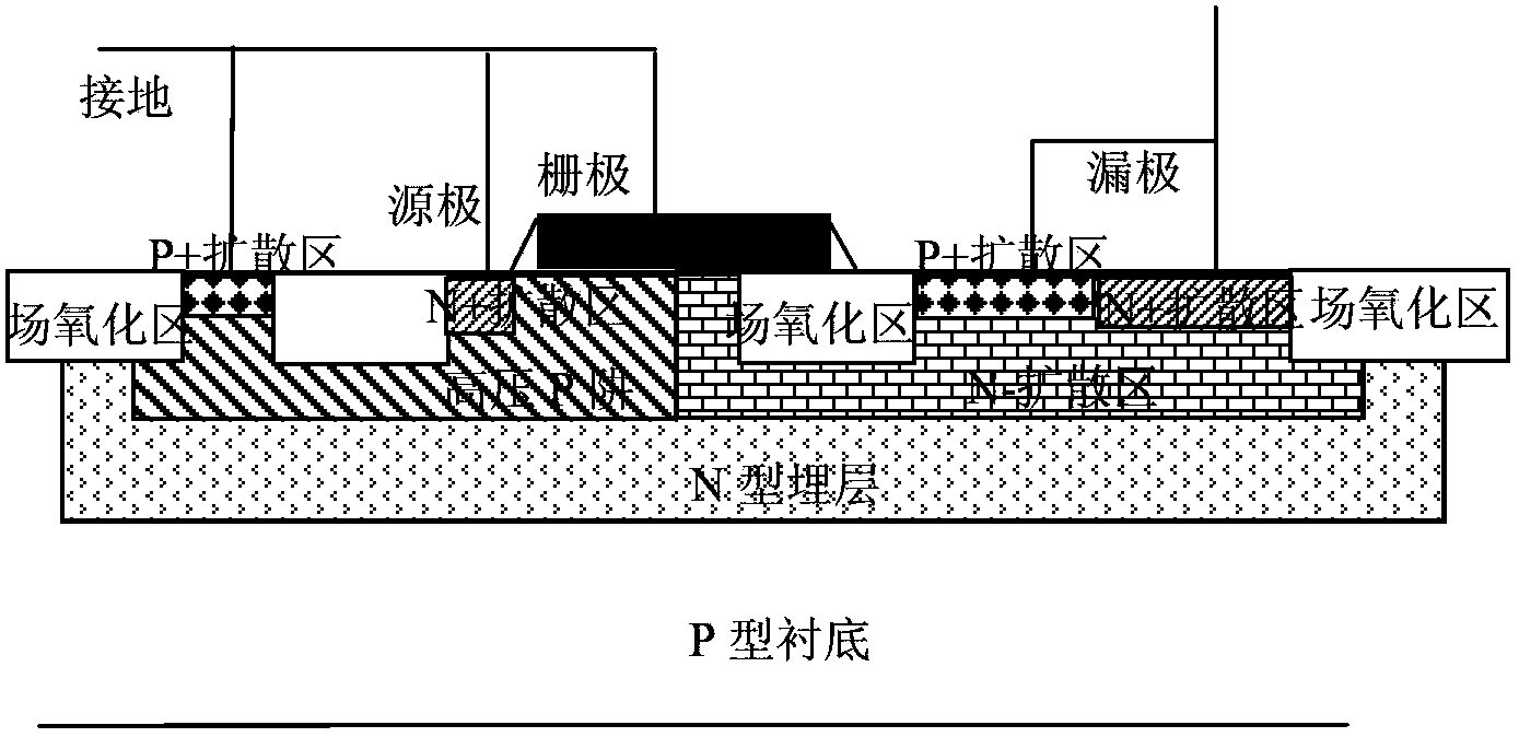
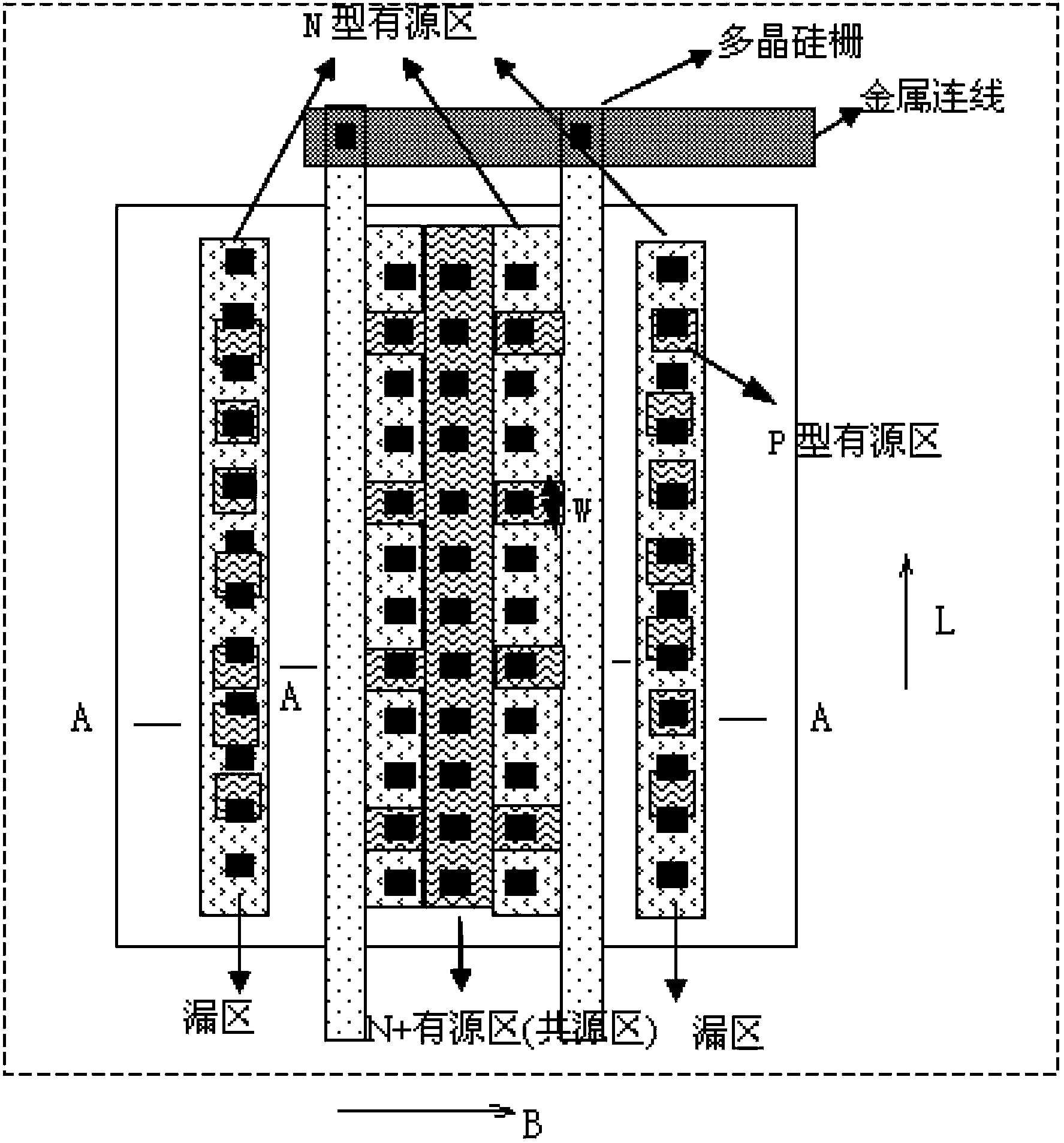
[0022] like image 3 As shown, the high-voltage NLDMOS structure used for electrostatic protection of the present invention includes an N-type LDMOS formed in an N-type buried layer above a silicon substrate; the N-type LDMOS is arranged in a multi-finger structure; located between two drain regions The source region between is the common source region, and the source region is the N+ active region;

[0023] The outermost is the drain region of LDMOS;

[0024] In the active region of the drain region, there are N-type active region and P-type active region along the length direction (ie image 3 in the L direction) are arranged alternately;

[0025] A P-type active region is inserted in the common source region, the P-type active region is embedded in the N-type active region, and the P-type active region separates the N-type active regions in the source region; the P-type active region and the N-type active regions are arranged alternately along the length direction to for...


PUM


Abstract

The invention discloses a high-voltage NLDMOS (N-type laterally diffused metal oxide semiconductor) structure for electrostatic protection. The high-voltage NLDMOS structure comprises an NLDMOS formed in an N-type buried layer above a silicon substrate. The NLDMOS is arranged to be a multi-finger structure. A source region between two drain regions is a joint source region. N-type active regions and P-type active regions are arranged at intervals along the length direction in active regions of the drain regions. The P-type active regions are inserted into the joint source region and embedded in the N-type active regions. The N-type active regions in the source region are separated respectively by the P-type active regions. The P-type active regions and the N-type active regions are arranged at intervals along the length direction. All drain electrodes are connected to an ESD (electro-static discharge) access end. All source electrodes are connected to the ground. All grid electrodes are connected to a signal end. By changing the width of a diffused region P+, close to the grid electrodes, on the source region, the high-voltage NLDMOS structure can effectively adjust trigger current and snapback voltage. By the high-voltage NLDMOS structure applied to high-voltage electrostatic protection, locking-resisting capability of an LDMOS (laterally diffused metal oxide semiconductor) can be effectively improved, and electrostatic protection capability of the LDMOS can be ensured not to be affected.

Description

technical field [0001] The invention relates to an electrostatic protection structure of a semiconductor device, in particular to a high-voltage NLDMOS structure for electrostatic protection. Background technique [0002] The existing high-voltage NLDMOS (N-type laterally diffused metal field effect transistor) structure for electrostatic protection is as follows: figure 1 As shown, under the occurrence of static electricity, after the ESD (electrostatic discharge) positive charge enters the drain from the input and output pads, the potential of the N- diffusion region will be raised, and an avalanche breakdown will occur; the breakdown current passes through the P+ diffusion in the P well The area is drawn out, and the potential of the P well is raised at the same time, causing the parasitic transistor to be turned on. The parasitic triode is a lateral triode composed of an N- diffusion region of the drain, an N+ diffusion region of the source and a high-voltage P well und...

Claims


Application Information

Patent Timeline
Patent Type & Authority Applications(China)
IPC IPC(8): H01L29/78H01L29/06H01L29/36
CPCH01L29/0684H01L29/7816
Inventor 苏庆苗彬彬王邦磷邓樟鹏
Owner SHANGHAI HUAHONG GRACE SEMICON MFG CORP
Why Eureka
Try Eureka