Structure of comprehensive type silicon epitaxy process photoetching alignment mark and manufacturing method

A technology of lithography alignment and silicon epitaxy, which is applied in semiconductor/solid-state device manufacturing, electrical components, electrical solid-state devices, etc., can solve the problems of deformation and disappearance of lithography alignment marks

Active Publication Date: 2014-02-12
SHANGHAI HUAHONG GRACE SEMICON MFG CORP
View PDF4 Cites 10 Cited by
  • Summary
  • Abstract
  • Description
  • Claims
  • Application Information

AI Technical Summary

Problems solved by technology

[0003] One of the technical problems to be solved by the present invention is to provide a method for making a comprehensive silicon epitaxial process lithography alignment mark, which can solve the problem of deformation and disappearance of the lithography alignment mark after epitaxial growth

Method used


Image

  • Structure of comprehensive type silicon epitaxy process photoetching alignment mark and manufacturing method
  • Structure of comprehensive type silicon epitaxy process photoetching alignment mark and manufacturing method
  • Structure of comprehensive type silicon epitaxy process photoetching alignment mark and manufacturing method

Examples


Embodiment Construction

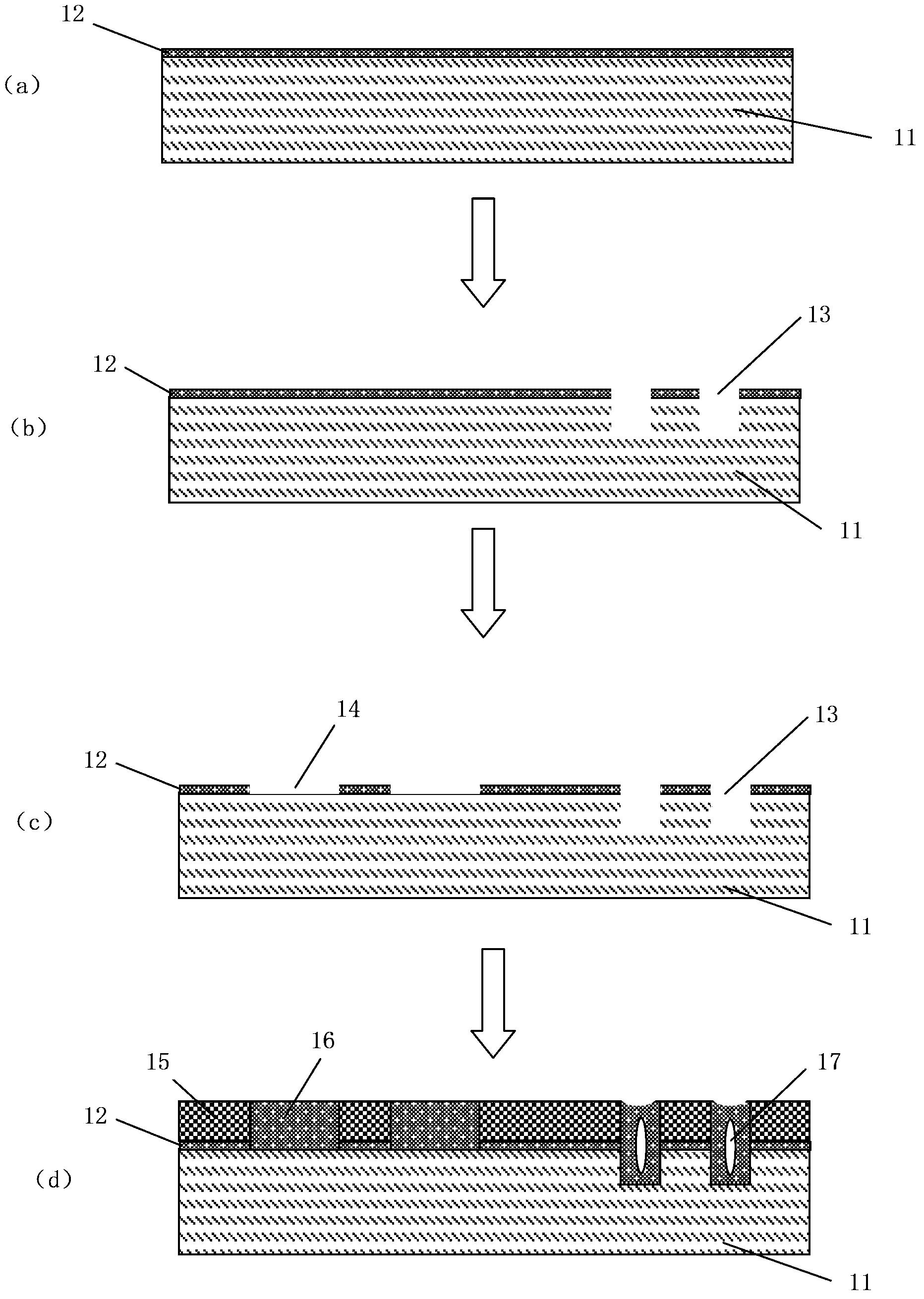
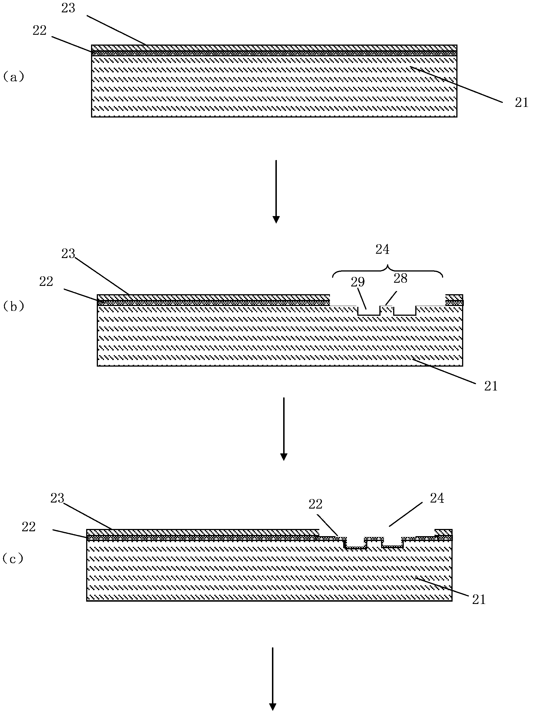
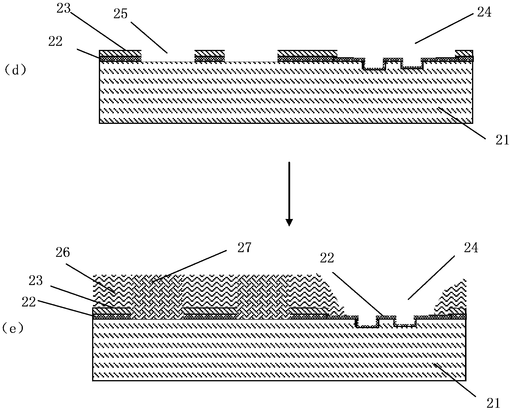
[0029] In order to have a more specific understanding of the technical content, characteristics and effects of the present invention, now in conjunction with the illustrated embodiment, the details are as follows:

[0030] The selective silicon epitaxy process refers to the growth of a single crystal on a silicon single crystal by adding a precursor containing chlorine atoms to the silicon source during the silicon epitaxial growth process, but not on a certain dielectric film. . Different dielectric films require different components of chlorine-containing precursors. Therefore, when multiple dielectric films exist on the same surface at the same time, silicon epitaxy can be grown on a certain dielectric film under a specific chlorine-containing precursor component. , while silicon epitaxy does not grow on other dielectric films.

[0031] Utilizing the characteristics of the above-mentioned selective silicon epitaxial process, the present invention has produced the lithograp...


PUM

PropertyMeasurementUnit
thicknessaaaaaaaaaa

Abstract

The invention discloses a manufacturing method of a comprehensive type silicon epitaxy process photoetching alignment mark. The manufacturing method comprises the steps that 1) a first dielectric film and a second dielectric film sequentially grow on a silicon substrate, wherein the first dielectric film is a film layer which can inhibit growth of silicon crystal, and the second dielectric film is a film layer which can inhibit growth of the first dielectric film on the surface of the substrate; 2) a photoetching alignment window and a photoetching alignment groove are etched; 3) the first dielectric film grows on the surface of the photoetching alignment window and the surface of the photoetching alignment groove; 4) a silicon single crystal window is etched; 5) comprehensive type silicon epitaxy growth is performed. The invention further discloses a structure of the photoetching alignment mark manufactured in the method. According to the structure of the comprehensive type silicon epitaxy process photoetching alignment mark and the manufacturing method, due to the fact that an epitaxy deposition process is regulated and a non-deposition area is formed on the surface of the photoetching alignment mark, the problem that the photoetching alignment mark deforms and disappears after epitaxy growth is solved.

Description

technical field [0001] The invention relates to the field of semiconductor integrated circuit manufacturing, in particular to a structure and a manufacturing method of a photolithographic alignment mark in a comprehensive silicon epitaxy process. Background technique [0002] The comprehensive silicon epitaxy process refers to the presence of semiconductor regions and dielectric film regions on the semiconductor surface. The silicon epitaxy process grows silicon single crystals in the semiconductor region, and grows silicon polycrystalline or silicon amorphous in the dielectric film region. The fabrication method of conventional full-scale silicon epitaxial process lithography alignment mark is (see figure 1 ): (1) growing a dielectric film 12 on a silicon substrate 11, such as figure 1 As shown in (a); (2) etching a photolithographic alignment groove 13, such as figure 1 As shown in (b); (3) etching out the single crystal window 14, such as figure 1 As shown in (c); (4) ...

Claims


Application Information

Patent Timeline
Patent Type & Authority Applications(China)
IPC IPC(8): H01L21/31H01L23/544
CPCH01L21/0338H01L23/544
Inventor 刘继全高杏
Owner SHANGHAI HUAHONG GRACE SEMICON MFG CORP
Why Eureka
Try Eureka