Device for bonding semiconductor chips

A semiconductor and chip technology, applied in semiconductor/solid-state device manufacturing, transportation and packaging, conveyor objects, etc., can solve problems such as material jams, scrapping, chip 10 scratches, etc.

Active Publication Date: 2014-02-12
苏州均华精密机械有限公司
View PDF3 Cites 10 Cited by
  • Summary
  • Abstract
  • Description
  • Claims
  • Application Information

AI Technical Summary

Problems solved by technology

The feeding jaws 17 are alternately transported to the discharge end in a relay manner, and the warping of the substrate 5 often causes the feeding jaws 17 to be incorrectly clamped and positioned when they are rep

Method used


Image

  • Device for bonding semiconductor chips
  • Device for bonding semiconductor chips
  • Device for bonding semiconductor chips

Examples


Example Embodiment

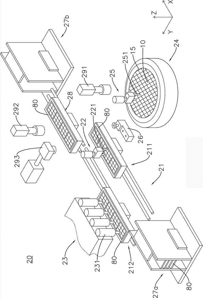
[0045] Example: see image 3 , Figure 4 , Figure 5 , Image 6 and Figure 7 Shown:
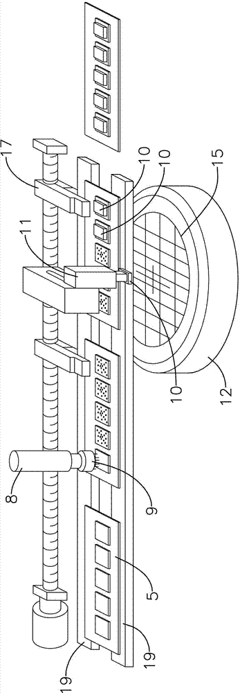
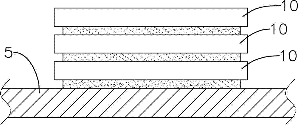
[0046] A device for adhering a semiconductor chip is used for adhering and fixing the chip 10 or stacking multiple chips 10 on a packaging carrier 80. The device for adhering semiconductor chips includes: a pre-compression module 22, which will take and place and apply pressure to pre-compress at least one chip 10 with a package carrier 80 or another chip 10 on a package carrier 80; and a main compression module 23. It includes a plurality of pressing heads 231, which simultaneously presses a plurality of pre-compressed chips 10, and causes the plurality of chips 10 to interact with a package carrier 80 or other chips 10 on a package carrier 80. Pressing; a first feeding and conveying mechanism 211; and a second feeding and conveying mechanism 212, the first feeding and conveying mechanism 211 and the second feeding and conveying mechanism 121 respectively convey the packaging carrier 80 to th...


PUM


Abstract

A device for bonding semiconductor chips is a packaging mechanism which is used for bonding and fixing the chips or used for stacking multiple chips. The device comprises a first feeding conveying mechanism, a second feeding conveying mechanism, a pre-pressing module and a main pressing fit module. A packaging carrier is conveyed to a position for performing pre-pressing fit of the pre-pressing module through the first feeding conveying mechanism and the second feeding conveying mechanism respectively, and the packaging carrier which has been processed in a pre-pressing fit is conveyed to or made to remain in the position for performing main pressing fit of the main pressing fit module respectively through the first feeding conveying mechanism and the second feeding conveying mechanism respectively. The pre-pressing module can apply pressure to enable at least one chip to be in pre-pressing fit with the packaging carrier or another chip on the packaging carrier. Then, the multiple chips which have been processed in a pre-pressing fit are stressed by multiple pressing-fit heads of the main pressing fit module at the same time, and thus the multiple chips are in main pressing fit with the packaging carrier or the chip on the packaging carrier.

Description

technical field [0001] The invention relates to a device for adhering semiconductor chips, in particular to a packaging device used in the die bonding process for making semiconductor electronic components. Background technique [0002] In the entire semiconductor packaging process, the process immediately after wafer dicing is the die bonding (or called die bonding, die attaching or die bonding) process, which is the process of cutting each independent chip on the wafer due to the dicing line. (or chip die) are sequentially picked and placed on the lead frame or the substrate, and the lead frame and the chip are firmly combined with each other by adhesive (eg: silver glue) or adhesive tape. [0003] figure 1 It is a schematic diagram of the main mechanism of an existing die bonding machine. The substrate 5 (substate) is loaded from the feed end on the left side of the conveyor rail 19 , and the substrates 5 loaded in sequence are transferred to the discharge end of the co...

Claims


Application Information

Patent Timeline
IPC IPC(8): H01L21/67H01L21/677
CPCH01L21/67092H01L21/67703H01L21/68
Inventor 石敦智
Owner 苏州均华精密机械有限公司
Why Eureka
Try Eureka