Printed circuit board and method for manufacturing a printed circuit board

A technology for printed circuit boards and manufacturing methods, applied in the directions of printed circuit manufacturing, printed circuits, printed circuits, etc., can solve the problems of uneven tin consumption, component offset, components cannot be accurately aligned, and reduce solder paste. The effect of layer area

Inactive Publication Date: 2014-02-12
WISTRON CORP
View PDF3 Cites 7 Cited by
  • Summary
  • Abstract
  • Description
  • Claims
  • Application Information

AI Technical Summary

Problems solved by technology

However, since the solder paste will melt into a liquid state during the hot air reflow process, once the solder paste is applied to a large area, the components above it will be seriously shifted, resulting in the inability of the components to be accurately aligned on the chip. area 114a, and there will also be problems such as uneven tin consumption

Method used


Image

  • Printed circuit board and method for manufacturing a printed circuit board
  • Printed circuit board and method for manufacturing a printed circuit board
  • Printed circuit board and method for manufacturing a printed circuit board

Examples


Embodiment Construction

[0025] In order to make the above and other objects, features and advantages of the present invention more comprehensible, specific embodiments of the present invention are listed below and described in detail in conjunction with the accompanying drawings.

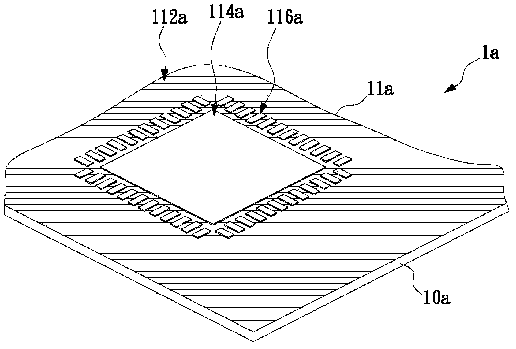
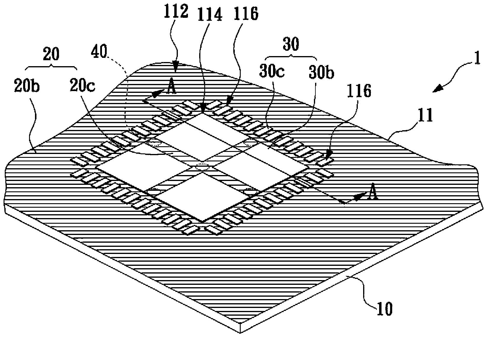
[0026] Please refer to the following figure 2 and image 3 The structure of the printed circuit board of the first embodiment of the present invention is schematically shown.

[0027] Such as figure 2 As shown, in one embodiment of the present invention, the printed circuit board 1 of the present invention includes a copper foil substrate 10, a solder resist layer 20, a solder paste layer 30 and at least one through hole 40, wherein the solder resist layer 20 includes a main anti- The solder layer 20b is isolated from the solder resist layer 20c, and the solder paste layer 30 includes a solder paste layer 30b in a sub-attachment area and a solder paste layer 30c in a pin area.

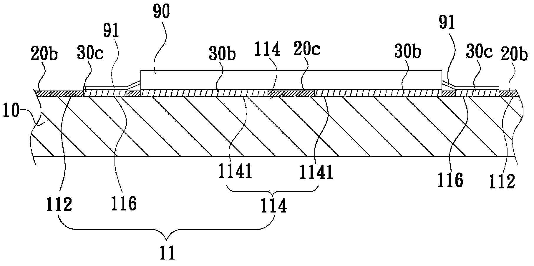
[0028] Such as figure 2 and image 3...


PUM


Abstract

A printed circuit board is disclosed. The printed circuit board includes a solder mask area and at least one chip attachment area. The at least one chip attachment area has an isolation solder mask layer such that the chip attachment area forms a plurality of chip sub-attachment areas to reduce an area of a solder paste smeared on the chip attachment area, and the isolation solder mask layer has at least one hole.

Description

technical field [0001] The invention relates to an improvement of a welding pad of a printed circuit board. Background technique [0002] Surface Mount Technology (SMT) is a process method for soldering electronic components to a printed circuit board. The soldering method is to apply solder paste to the solder pad (Pad) on the printed circuit board, and then Then use a mounting machine to place components (such as IC chips, transistors, etc.) on the solder pads coated with solder paste, and finally go through hot air reflow to melt the solder paste and combine the components with the printed circuit board. [0003] Due to the demands of high speed and thinness of current electronic products, the heat dissipation of components has become a major issue. Taking a chip made of a quad flat no leads (QFN) package as an example, in order to have a good heat dissipation effect, the thermal pad has a large area. Relatively speaking, its The corresponding pad area will be large. ...

Claims


Application Information

Patent Timeline
Patent Type & Authority Applications(China)
IPC IPC(8): H05K1/18H05K3/34
CPCH05K1/0209H05K3/3421H05K3/3452H05K2201/09063H05K2201/10969Y02P70/50H05K3/0073H05K1/092
Inventor 詹荣明吕慧玲徐淑婷范睿昀周慧莹
Owner WISTRON CORP
Why Eureka
Try Eureka