
Semiconductor device

A semiconductor and device technology, applied in the field of packaging semiconductor devices, to achieve high reliability, reduce thermal stress, and reduce packaging costs

Inactive Publication Date: 2014-02-12
NODA SCREEN
View PDF4 Cites 4 Cited by
  • Summary
  • Abstract
  • Description
  • Claims
  • Application Information

AI Technical Summary

Problems solved by technology

This structure creates the following problems

Method used


Image

  • Semiconductor device
  • Semiconductor device
  • Semiconductor device

Examples


Embodiment Construction

[0049] refer to Figure 1 to Figure 9 A first embodiment of the present invention is described.

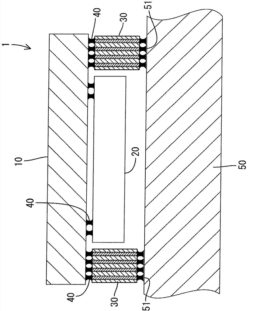
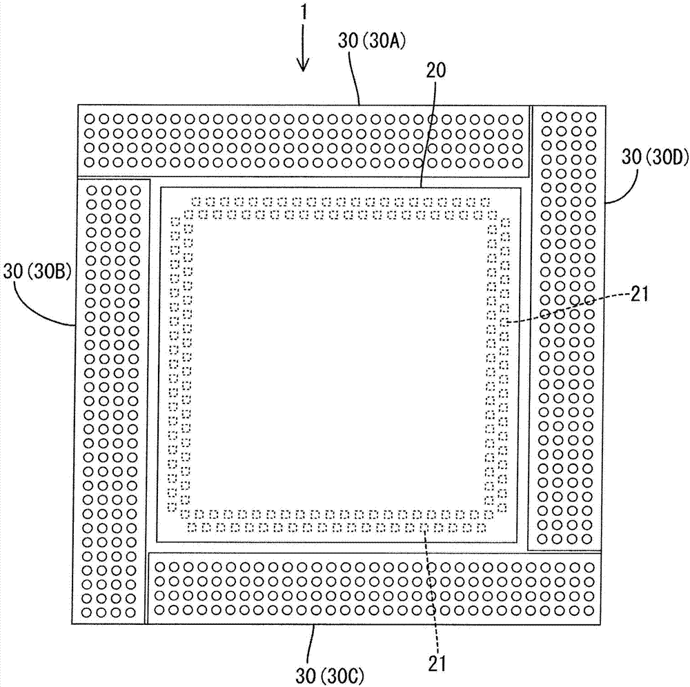
[0050] 1. Structure of semiconductor device

[0051] figure 1 is a schematic cross-sectional view showing the semiconductor device 1 of the first embodiment. The semiconductor device 1 includes an interposer 10 , a semiconductor chip 20 and a plurality of stud arrays 30 . The semiconductor device is packaged by connecting the semiconductor chip 20 and the post array 30 to one (lower) surface of the interposer 10 by means of reflowed solder 40 . The packaged semiconductor device 1 is mounted on a known printed wiring board 50 through a post array 30 . The printed wiring board 50 includes an organic material (resin), for example, the printed wiring board is made of glass epoxy resin.

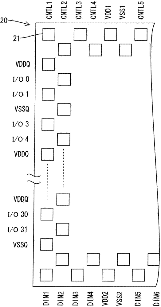
[0052] The semiconductor chip 20 has a known configuration including a silicon substrate and a predetermined semiconductor integrated circuit (not shown). Semiconductor integrated circuits are p...


PUM


Abstract

This semiconductor device is provided with a semiconductor chip, a relay substrate, a surface circuit pattern, and a post array. The surface circuit pattern is configured of: a chip-side pad group, which is formed on one surface of the relay substrate, and which is connected to the external connection pads of the semiconductor chip; a relay wiring group, which is laid to extend to the outer peripheral side of the relay substrate by being connected to the chip-side pad group; and a relay pad group, which is connected to the relay wiring end portions on the side opposite to the chip-side pads. In the post array, a plurality of conductive paths are formed to extend in the direction intersecting the surface of the relay substrate, the conductive paths are in a state of being insulated from each other by means of an insulating resin, the end portions of the conductive paths, said end portions being on the relay substrate side, are connected to the relay pads, and conductive path end portions on the side opposite to the relay substrate are connected to the printed board side.

Description

technical field [0001] The present invention relates to a packaged semiconductor device including a semiconductor chip. Background technique [0002] In recent years, this type of semiconductor device has been increasingly expected to have a smaller size. For example, a package of a semiconductor chip mounted on a printed wiring board made of an organic material such as a motherboard and an interposer integrated with each other, that is, a CSP structure, is actually employed. [0003] The semiconductor device in Patent Document 1 is an example of a CSP structure including a package in which a semiconductor chip is connected to an interposer made of an organic material (resin). The interposer has a plurality of through holes, and the solder balls are exposed on the upper and lower surfaces of the interposer through the through holes. The external connection pads provided on the semiconductor chip are connected to the upper ends of the terminals of the interposer. The lower...

Claims


Application Information

Patent Timeline
Patent Type & Authority Applications(China)
IPC IPC(8): H01L23/12H05K1/14
CPCH05K1/14H01L23/12H01L23/49827H01L23/50H01L2224/14133H01L2924/171H01L24/06H01L2224/16227H01L2224/81815H01L2224/14135H01L2225/0652H01L23/60H01L23/64H01L25/0652H01L25/0657H01L2225/06572H05K1/141H05K3/368H05K2201/10378H05K2201/10515H05K2201/2036H01L2924/12032H01L2224/05554H01L2924/15321H01L2224/0401H01L2924/351H01L2924/15788H01L23/147H01L23/15H01L23/49833H01L23/49838H01L2224/16225H01L2924/12036H01L2924/00014H01L2924/00H01L23/48H01L24/07H01L23/49822
Inventor 小山田成圣吉泽正充小川裕誉
Owner NODA SCREEN
Learn More