
A fast photodetector

A photodetector and fast technology, applied in the direction of electric solid devices, circuits, electrical components, etc., can solve the problems of complex structure design, affecting response speed, eliminating slow carriers, etc. remove the effect of the condition

Inactive Publication Date: 2016-08-31
UNIV OF ELECTRONICS SCI & TECH OF CHINA
View PDF4 Cites 0 Cited by
  • Summary
  • Abstract
  • Description
  • Claims
  • Application Information

AI Technical Summary

Problems solved by technology

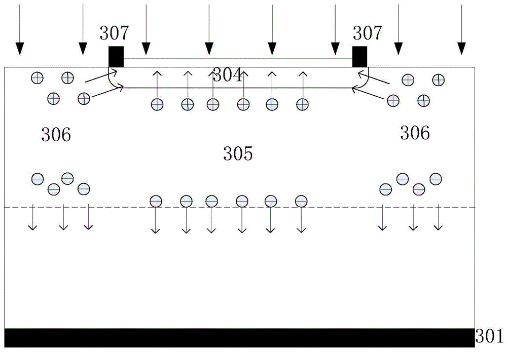
This structure has a better effect in solving the problem of vertical photogenerated carriers, but since photogenerated carriers also exist on the side of the N+ injection, these carriers cannot flow away quickly due to the distance from the electrode, which will affect the overall performance. responding speed
[0005] In summary, the method of improving the response speed of the photodetector by modifying the structure of the photodetector is complicated in structural design and cannot fundamentally eliminate the conditions for the generation of slow carriers.

Method used


Image

  • A fast photodetector
  • A fast photodetector
  • A fast photodetector

Examples


Embodiment 1

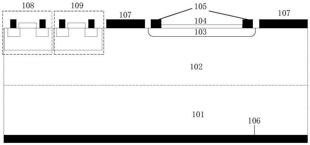
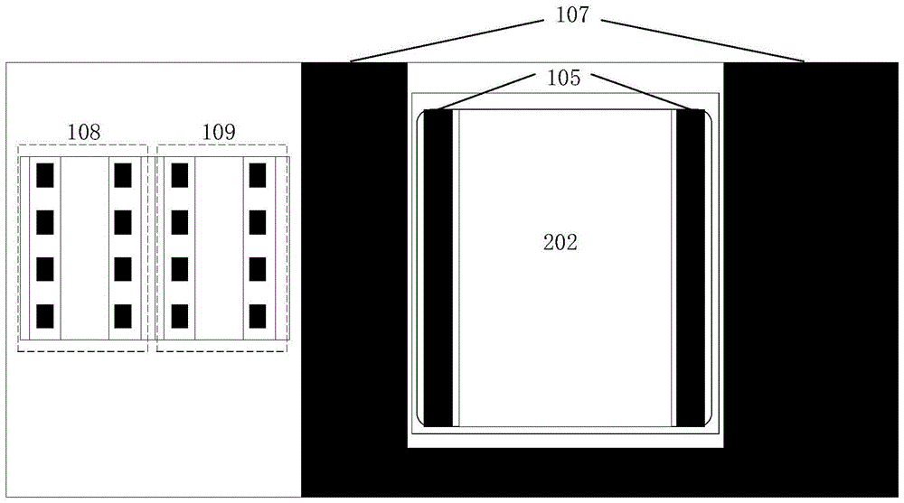
[0019] Such as figure 1 As shown, the photodetector of this example is manufactured using a vertical CMOS process, wherein the photodiode adopts a vertical structure and is fabricated on an N+ substrate 101 as the cathode of the phototube, and an N- epitaxial layer 102 is formed above the substrate. A layer of P+ injection region 103 is carried out in the epitaxy as the anode of the photoelectric tube, and a layer of anti-reflection film 104 is covered above the P+ injection region 103 to improve the light absorption efficiency of the photoelectric tube. The anode metal electrode 105 and the cathode metal electrode 106 are respectively Made on the surface and back of the photodiode, the metal covering area 107 and the anode metal electrode 105 adopt the same layer of metal version, covering around the photodiode, without any potential. The amplifying circuit is composed of several NMOS transistors 108 and PMOS transistors 109, which are interconnected with photodiodes through ...


PUM


Abstract

The invention relates to the technology of electronic components, in particular to a fast photoelectric detector. The fast photodetector of the present invention comprises a connected photodiode and an amplifying circuit, the photodiode includes an N+ substrate 101, an N-epitaxial layer 102, an anode metal electrode 105 and a cathode metal electrode 106, and the N- The epitaxial layer 102 is arranged on the upper end surface of the N+ substrate 101, the N-epitaxial layer 102 is provided with a P+ implantation region 103, and the upper end surface of the P+ implantation region 103 is provided with an anti-reflection film 104 and an anode metal electrode 105, so The amplifying circuit is composed of a plurality of NMOS transistors 108 and PMOS transistors 109, and it is characterized in that a light-shielding layer is arranged between the photodiode and the amplifying circuit, and the light-shielding layer is used for light-shielding the non-photosensitive area. The invention has the beneficial effects of fundamentally eliminating the generation conditions of slow photogenerated carriers, thereby greatly improving the response speed of the photodetector. The invention is particularly applicable to photodetectors.

Description

technical field [0001] The invention relates to the technology of electronic components, in particular to a fast photoelectric detector. Background technique [0002] A photodetector is a photodetection device made using the photoelectric effect of semiconductor materials. When the photodetector receives light, the photon carrying energy enters the PN junction of the photodiode, transfers the energy to the bound electrons on the covalent bond, and makes some electrons break free from the covalent bond, thereby generating electron-hole pairs, which are called electron-hole pairs. Photogenerated carriers, they participate in the drift movement under the action of the reverse voltage, thereby generating a reverse current, called photocurrent, if the load is connected to the external circuit, the load will obtain an electrical signal, thus realizing the transformation from optical signal to Conversion of electrical signals. These carriers are generated at different positions. ...

Claims


Application Information

Patent Timeline
Patent Type & Authority Patents(China)
IPC IPC(8): H01L27/06H01L31/0232H01L31/103
Inventor 张有润董梁孙成春张飞翔刘影张明高向东张波
Owner UNIV OF ELECTRONICS SCI & TECH OF CHINA
Learn More