Silicon carbide seed crystal bonding device

A silicon carbide seed and bonding technology, applied in the direction of single crystal growth, crystal growth, single crystal growth, etc., can solve problems such as crystal cracking

Inactive Publication Date: 2014-02-26
HEBEI SYNLIGHT CRYSTAL CO LTD
View PDF4 Cites 17 Cited by
  • Summary
  • Abstract
  • Description
  • Claims
  • Application Information

AI Technical Summary

Problems solved by technology

[0004] The technical problem to be solved by the present invention is to provide a silicon carbide seed crystal bonding device to solve the problem of severe stress and crystal cracks caused by the difference in the expansion coefficients of graphite and silicon carbide single crystal during the cooling process of crystal growth

Method used


Image

  • Silicon carbide seed crystal bonding device

Examples


Embodiment Construction

[0015] The principles and features of the present invention are described below in conjunction with the accompanying drawings, and the examples given are only used to explain the present invention, and are not intended to limit the scope of the present invention.

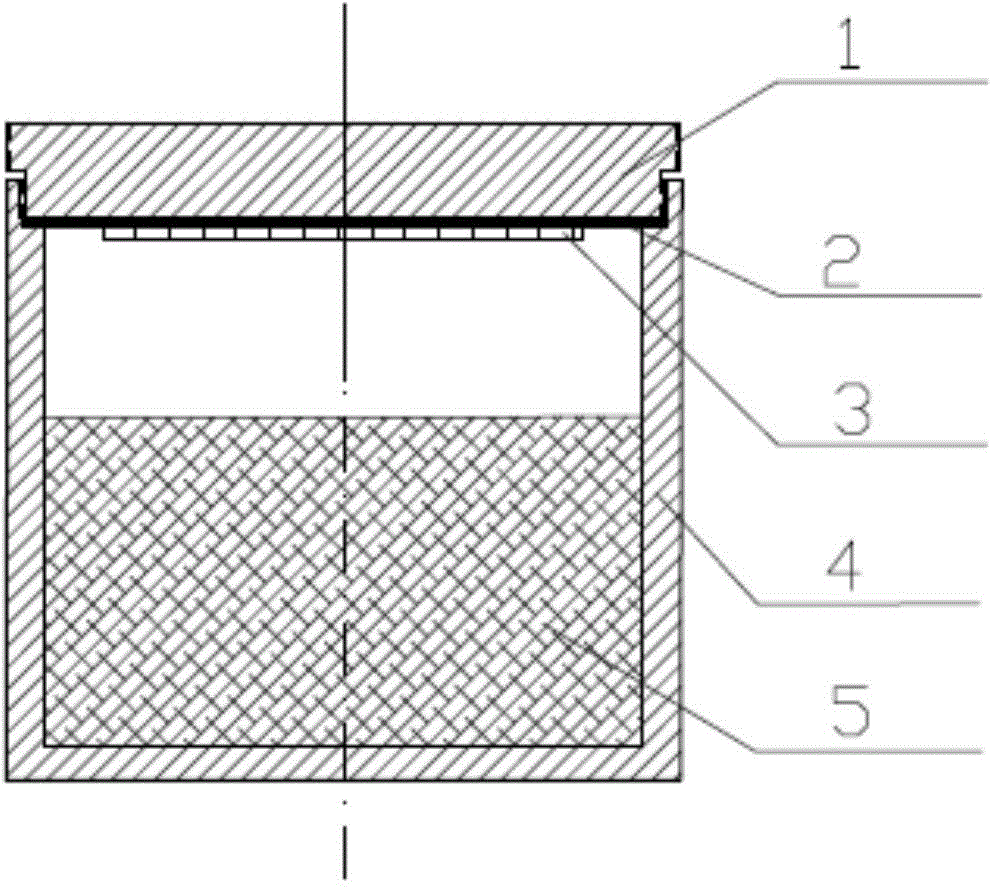
[0016] figure 1 It is a structural schematic diagram of the first specific embodiment of a seed crystal bonding device of the present invention, such as figure 1 As shown, in the first specific embodiment, the seed crystal bonding device provided by the present invention includes a graphite cover (1) and a seed crystal bonding plate (2), and the seed crystal (3) is bonded to the seed crystal The connecting plate (2) is bonded, the graphite cover (1) and the seed crystal bonding plate (2) are bonded, the thickness of the seed crystal bonding plate (2) is equal to 2 mm, and the material of the seed crystal bonding plate (2) is graphite. In this embodiment, the seed crystal bonding plate ( 2 ) is molded graphite, and ...


PUM

PropertyMeasurementUnit
thicknessaaaaaaaaaa
thicknessaaaaaaaaaa
thicknessaaaaaaaaaa

Abstract

The invention provides a silicon carbide seed crystal bonding device comprising a graphite cover and a seed crystal bonding plate, wherein a seed crystal is bonded together with the seed crystal bonding plate, the graphite cover is fixedly connected with the seed crystal bonding plate, and the thickness of the seed crystal bonding plate is smaller than or equal to 2mm. According to the invention, the original seed crystal bonding graphite plate is divided into two parts, the seed crystal is bonded by using the seed crystal bonding plate with smaller thickness, and after the crystal growth is finished and the temperature is reduced, the seed crystal bonding plate is thinner and can deform, so that the stress in the crystal can be effectively released, and the breakage rate of the crystal and a wafer can be reduced.

Description

technical field [0001] The invention relates to the field of crystal growth, in particular to a silicon carbide seed crystal bonding device. Background technique [0002] As a third-generation semiconductor material, silicon carbide has excellent physical and chemical properties, which determines that silicon carbide has broad application prospects and market space in high-end optoelectronics, high-power, microwave radio frequency and other fields. However, the high-density defects contained in silicon carbide single crystal substrates will greatly affect the actual performance of various silicon carbide-based devices, and even lead to device failure. Therefore, it is very necessary and important to study the defects of SiC single crystal substrates. [0003] Silicon carbide material is a crystal with a large elastic modulus. The growth of silicon carbide crystals by PVT (physical vapor transport method) method needs to be above 2000 ° C. Generally, the crystal growth is th...

Claims


Application Information

Patent Timeline
Patent Type & Authority Applications(China)
IPC IPC(8): C30B23/00C30B29/36
Inventor 陶莹高宇邓树军赵梅玉段聪
Owner HEBEI SYNLIGHT CRYSTAL CO LTD
Why Eureka
Try Eureka