Unlock instant, AI-driven research and patent intelligence for your innovation.

Multipoint positioning method for wafer macroscopic defect

A multi-point positioning, macro defect technology, applied in the direction of optical testing flaws/defects, measuring devices, instruments, etc., can solve problems such as consumption, inability to find, waste of inspection time, etc., to improve inspection efficiency, save time, and improve inspection speed. Effect

Inactive Publication Date: 2014-02-26
SHANGHAI HUALI MICROELECTRONICS CORP
View PDF6 Cites 8 Cited by
  • Summary
  • Abstract
  • Description
  • Claims
  • Application Information

AI Technical Summary

Problems solved by technology

However, after zooming in on the coordinate points located under the macroscopic view, the defect may not be found within the field of view 4, such as figure 2 Shown is the field of view after zooming in on the macroscopic positioning point. The slash area is the visible field of view 4, and the black dot is the wafer defect 1. Due to the large error between the positioning point and the actual coordinate point of the defect under macroscopic conditions, there may be a large error when zooming in. After 4 times the defect may not be found in the field of view, and then it needs to be adjusted to observe the specific orientation of the defect. Since the visible range on the wafer is small under microscopic conditions, if no defect is found under microscopic conditions, it is necessary to It takes a long time to find the defect and locate it, which takes a long time to detect
[0006] Chinese patent (CN102269712A) discloses a wafer defect detection method. By generating a simulated wafer consistent with the tested wafer, the position of the chip on the tested wafer is completely aligned with the position of the chip on the simulated wafer. The position information of the chip on the chip is processed, and the specific moving distance of the optical microscope operating table in the horizontal axis direction and the vertical axis direction is controlled according to the processing result, so that the optical microscope can be accurately aligned with the position of each tested chip on the tested wafer, and the solution It solves the problem that mistakes are often made when determining each inspected chip scattered in different positions of the wafer through pure visual inspection, which will affect the accuracy of the final inspection result, and effectively improves the work efficiency of wafer defect inspection.
[0007] However, in the process of wafer inspection, it is necessary to perform macro inspection first and then micro inspection. Since there may be a large difference between the coordinate points positioned during a single macro inspection and the real coordinates of defects, and then it takes more time to perform micro inspection. Long time to find defects, wasting a lot of inspection time

Method used


Image

  • Multipoint positioning method for wafer macroscopic defect
  • Multipoint positioning method for wafer macroscopic defect
  • Multipoint positioning method for wafer macroscopic defect

Examples


Embodiment Construction

[0026] The specific embodiment of the present invention will be further described below in conjunction with accompanying drawing:

[0027] The invention provides a method for multi-point positioning of wafer macroscopic defects, comprising the following steps:

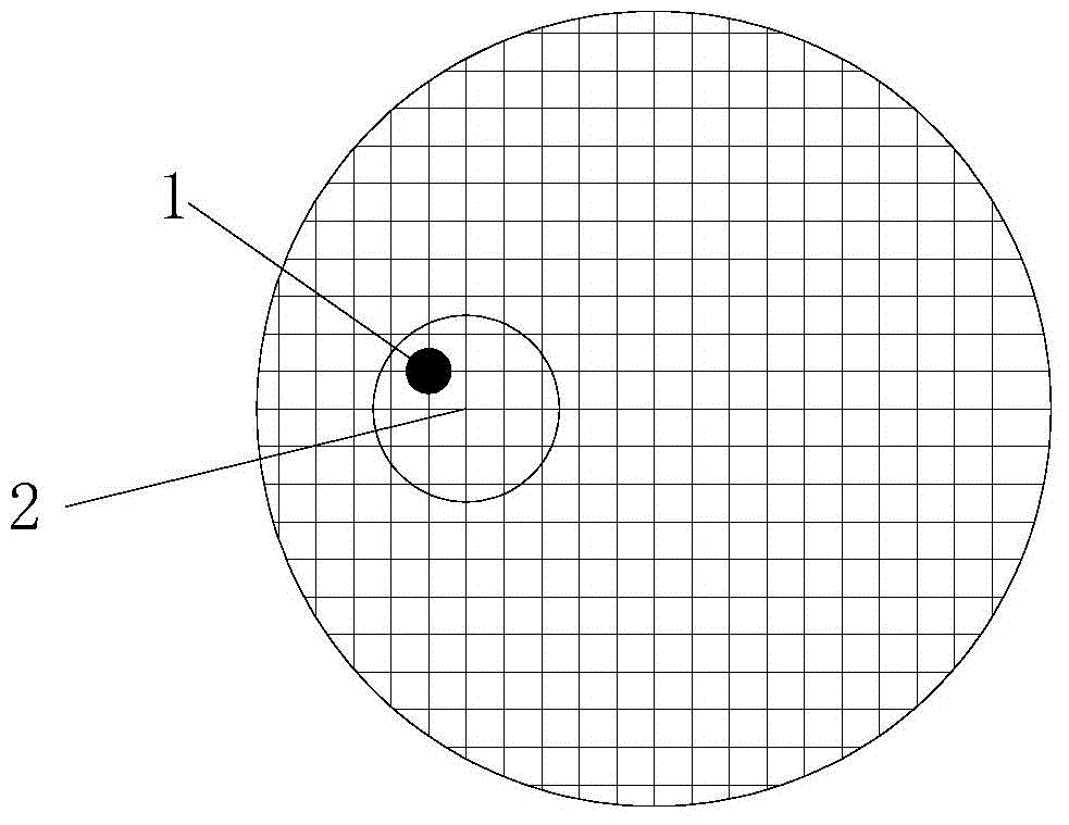
[0028] Provide a wafer that needs to be inspected for defects. First, take a photo of the wafer with macro defects in the macro monitoring area of ​​the Nikon OST3200 microscope. This photo can capture the entire wafer surface. If there are no visible defects in the photo, proceed to other processes; if there are visible defects, then find macro defect 1 on this photo, and perform multiple (more than 10) positioning near this defect, and record the coordinates of each positioning point Then add the horizontal and vertical coordinate values ​​of each positioning point respectively, and then divide them by the number of positioning times to obtain the average coordinate of multiple positioning coordinate values, and calc...


PUM


Abstract

A provided multipoint positioning method for wafer macroscopic defect comprises the following steps: photographing wafer surface, performing multi-time positioning on macroscopic visible defect vicinity, recording coordinate figures of each time positioning; utilizing algorithm to perform calculation on the coordinate figures of the multi-time positioning to obtain an average coordinate figure; and directly performing microscopic detection by taking the average value as the coordinate figure to rapidly obtain the coordinate figure of the defect. The multipoint positioning method helps to reduce the error by utilizing multi-time positioning and then averaging, helps to rapidly find the position of the defect and perform positioning under the microscopic condition, and helps to substantially improve the detection efficiency.

Description

technical field [0001] The invention relates to the field of semiconductor testing, in particular to a multi-point positioning method for wafer macro defects. Background technique [0002] With the development of modern technology, semiconductors follow the development of "Moore's Law", the number of transistors that can be accommodated on an integrated circuit will double every 18 months, the performance of devices is getting higher and higher, and chips are also gradually miniaturized. Development, following Intel's announcement of 22nm technology and Samsung's announcement of 20nm technology, IBM announced in 2012 that it has mastered 9nm technology. As the device is getting smaller and its integration is getting higher and higher, it is necessary to perform wafer defect detection on the device. Avoid its defects from causing device failure. [0003] At present, the inspection of wafers is carried out by combining macroscopic and microscopic methods. Both actions can be ...

Claims


Application Information

Patent Timeline
IPC IPC(8): G01N21/95G01B11/00
Inventor 瞿丹红姜舜陈丽娟
Owner SHANGHAI HUALI MICROELECTRONICS CORP
Features
  • R&D
  • Intellectual Property
  • Life Sciences
  • Materials
  • Tech Scout
  • Unparalleled Data Quality
  • Higher Quality Content
  • 60% Fewer Hallucinations
Learn More