
Flexible display module manufacturing method and flexible display module through method

A technology for flexible displays and manufacturing methods, applied in semiconductor/solid-state device manufacturing, semiconductor devices, electric solid-state devices, etc., can solve the problem of poor crystallization of low-temperature polysilicon layer 700, affecting the curling performance of flexible thin-film transistor substrates, and large stress, etc. problems, to achieve the effect of reducing internal stress, avoiding influence, and facilitating thinning

Active Publication Date: 2014-02-26
TCL CHINA STAR OPTOELECTRONICS TECH CO LTD
View PDF11 Cites 10 Cited by
  • Summary
  • Abstract
  • Description
  • Claims
  • Application Information

AI Technical Summary

Problems solved by technology

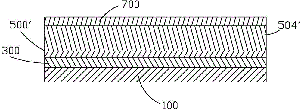
Although this method reduces the probability of deformation of the flexible substrate 300 to a certain extent, because the thickness of the silicon oxide layer 504' is too large, it will cause excessive stress and affect the curling performance of the flexible thin film transistor substrate. At the same time, it may also cause problems such as poor crystallization of the low-temperature polysilicon layer 700

Method used


Image

  • Flexible display module manufacturing method and flexible display module through method
  • Flexible display module manufacturing method and flexible display module through method
  • Flexible display module manufacturing method and flexible display module through method

Examples


Embodiment Construction

[0030] In order to further illustrate the technical means adopted by the present invention and its effects, the following describes in detail in conjunction with preferred embodiments of the present invention and accompanying drawings.

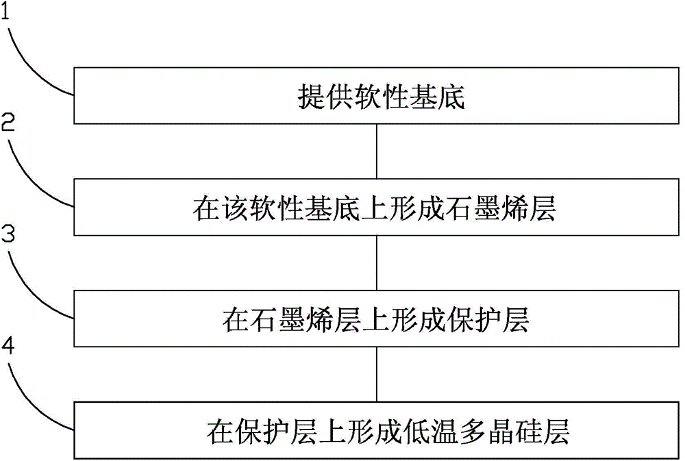
[0031] see image 3 and Figure 4 , the invention provides a method for manufacturing a flexible display assembly, comprising the following steps:

[0032] Step 1, providing a soft base 22 .

[0033] The flexible substrate 22 is made of polyethylene terephthalate (PET), polyethylene naphthalate (PEN), or polyimide (PI). In this embodiment, the flexible base 22 is formed on the glass substrate 20 .

[0034] Step 2, forming a graphene layer 24 on the flexible substrate 22 .

[0035] The graphene layer 24 is formed on the soft substrate 22 by microwave chemical vapor deposition (micro wave CVD), transfer or spin coat process. Graphene is a material with a single-layer sheet structure composed of carbon atoms. Graphene with a three-dimensiona...


PUM


Abstract

The invention provides a flexible display module manufacturing method and a flexible display module through the method. The method includes the first step of providing a flexible substrate (22), the second step of forming a graphene layer (24) on the flexible substrate (22), the third step of forming a protection layer (26) on the graphene layer (24), and the fourth step of forming a low-temperature polycrystalline silicon layer (28) on the protection layer (26). According to the flexible display module manufacturing method and the flexible display module through the method, the graphene layer is formed on the flexible substrate, so that heat produced in the process of manufacturing the low-temperature polycrystalline silicon layer is effectively led out, and then the influence of the heat on the flexible substrate is avoided. Meanwhile, the thickness of the protection layer does not need increasing, internal stress is reduced, and thinness of the flexible display module is facilitated.

Description

technical field [0001] The invention relates to the display field, in particular to a method for manufacturing a flexible display component and the fabricated flexible display component. Background technique [0002] With the vigorous development of display technology and information products, displays have entered the era of flat panel display (FPD) from traditional cathode ray tubes (cathode ray tubes, CRT). Compared with the existing rigid glass panel flat-panel display, the flexible display is safer because it is thinner, more flexible, and impact-resistant, and it is not restricted by occasions and spaces. It has become the next generation The new trend of display development. [0003] Flexible thin film transistor (thin film transistor, TFT) substrate is one of the important components of flexible displays, and the selection and development of its substrate material is the most important issue in the development of flexible displays. At present, the choices of flexib...

Claims


Application Information

Patent Timeline
Patent Type & Authority Applications(China)
IPC IPC(8): H01L21/77H01L27/12
CPCH01L21/02422H01L21/02444H01L21/02488H01L21/02499H01L21/02502H01L21/02532H01L27/1218H01L27/1262H01L29/1606H01L29/78603H01L27/1222H01L27/1285H01L29/78606H01L29/78675
Inventor 胡国仁
Owner TCL CHINA STAR OPTOELECTRONICS TECH CO LTD
Learn More