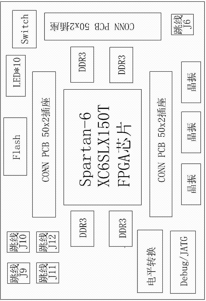
FPGA core circuit board structure
A core circuit and board structure technology, applied in electrical digital data processing, instruments, digital data processing components, etc., can solve the problems of poor scalability, low cost performance, high cost, etc., to achieve high data throughput and rich circuit structure. perfect effect
- Summary
- Abstract
- Description
- Claims
- Application Information
AI Technical Summary
Problems solved by technology
Method used
Image
Examples
Embodiment Construction
[0013] Such as figure 1 As shown in the figure, an FPGA core circuit board structure includes a circuit board. The circuit board is equipped with FPGA chips, four DDR3 chips, Flash chips, three crystal oscillator chips, level conversion chips, Debug / JATG interfaces, and five sets of jumpers. Line, a four-position switch, LED indicator light, three rows of 50x2 sockets; FPGA chip model is Spartan-6 XC6SLX150T, package is FGG676, the chip has many programmable resources and IO pins, the price is not high, and the price is relatively high; FPGA chip Four pieces of DDR3 with a capacity of 1Gb are connected around as storage memory. Each piece of DDR3 memory uses 15 address lines as address input, 16 data lines as data output, and 14-bit control signal lines. Four DDR3 pieces can read data in parallel at the same time. Large data throughput and high bandwidth. DDR3 has a high external data transfer rate and advanced address / command and control bus topology. Using DDR3 memory can red...
PUM
 Abstract
Description
Claims
Application Information
 - R&D
- Intellectual Property
- Life Sciences
- Materials
- Tech Scout
- Unparalleled Data Quality
- Higher Quality Content
- 60% Fewer Hallucinations
Browse by: Latest US Patents, China's latest patents, Technical Efficacy Thesaurus, Application Domain, Technology Topic, Popular Technical Reports.
© 2025 PatSnap. All rights reserved.Legal|Privacy policy|Modern Slavery Act Transparency Statement|Sitemap|About US| Contact US: help@patsnap.com

