Semiconductor storage device
A storage device and semiconductor technology, applied in the direction of information storage, static memory, digital memory information, etc., can solve the problem of reducing the power supply voltage of the storage unit, and achieve the effect of reliable storage and preservation
- Summary
- Abstract
- Description
- Claims
- Application Information
AI Technical Summary
Problems solved by technology
Method used
Image
Examples
no. 1 approach
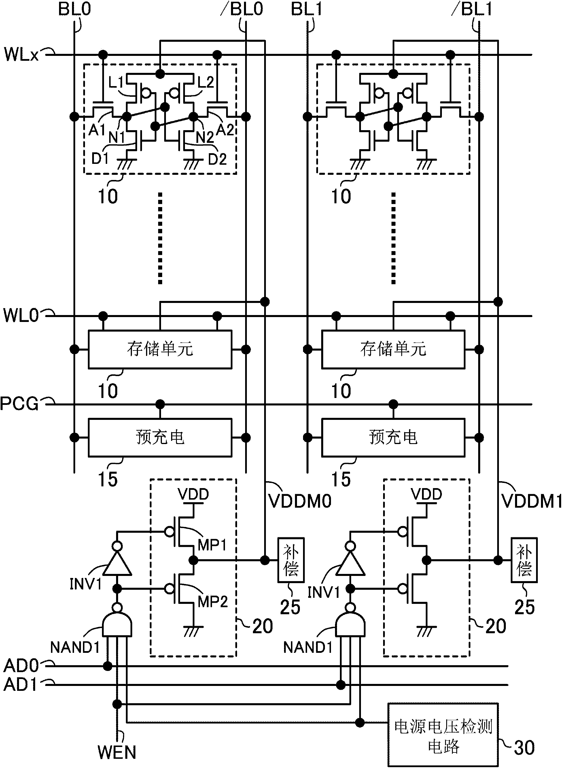
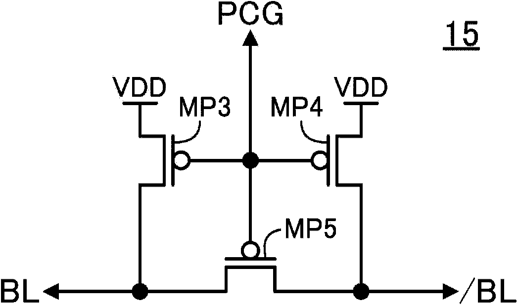
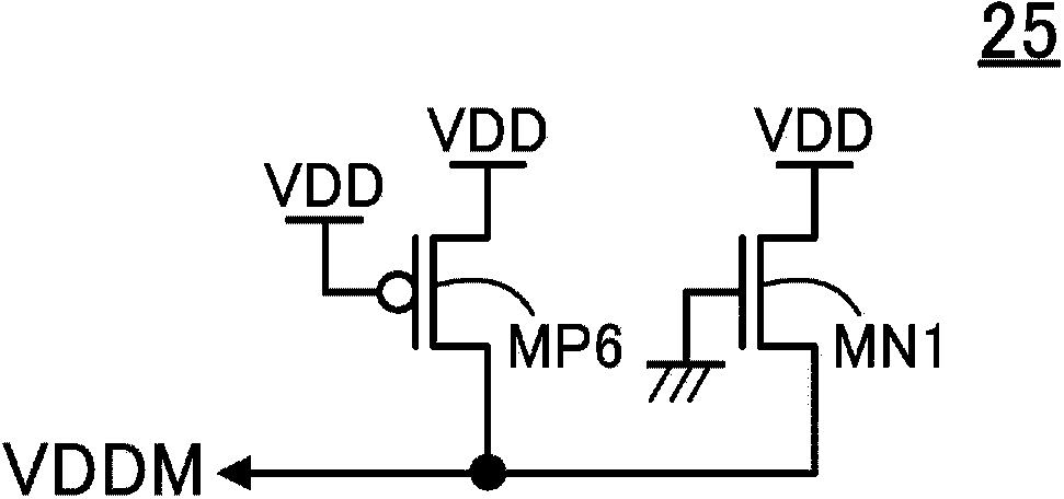
[0034] figure 1 It is a configuration diagram of the semiconductor memory device according to the first embodiment of the present invention. figure 1 The shown semiconductor storage device includes: a memory cell 10 composed of access transistors A1-2, drive transistors D1-D2, and load transistors L1-2 to have two storage nodes N1-2, a bit line precharge circuit 15, A memory cell power supply circuit 20 composed of P-type MOS transistors MP1-2, a leakage current compensation circuit 25, a power supply voltage detection circuit 30, an inverter circuit INV1, and a NAND circuit NAND1. WL0-x indicates word line, BL0-1 and / BL0-1 indicate bit line, PCG indicates precharge control signal, VDDM0-1 indicates memory cell power supply, AD0-1 indicates column address signal, WEN indicates write control signal, VDD Indicates a power source (first power source). X is an integer greater than 1, figure 1 A case where there are a plurality of memory cells 10 connected to a plurality of wor...
no. 2 approach
[0139] Figure 9 It is a configuration diagram of a semiconductor memory device according to a second embodiment of the present invention. Figure 9 The shown semiconductor memory device is compared to that in the first embodiment figure 1 The structure shown differs only in the structure of the MOS transistors constituting the memory cell power supply circuit 21 . Specifically, an N-type MOS transistor MN2 is added between the P-type MOS transistor MP2 and the ground power supply. Furthermore, the gate terminal of the P-type MOS transistor MP2 is connected to the drain terminal of the N-type MOS transistor MN2, and the same signal as that input to the gate terminal of the P-type MOS transistor MP1 is input to the gate terminal of the N-type MOS transistor MN2. Extreme.
[0140] Except when a write operation is being performed, the write control signal WEN is at L level (inactive state).
[0141] Therefore, regardless of the state of the column address signals AD0 and AD1,...
no. 3 approach
[0148] Figure 10 is a configuration diagram of a semiconductor memory device according to a third embodiment of the present invention. Figure 10 The shown semiconductor memory device is compared to the first embodiment figure 1 In terms of the structure, only the control of the memory cell power supply circuit 20 is different. Specifically, the point of difference is that the signal line of the write control signal WEN is connected to the gate terminals of the P-type MOS transistors MP1 of all the memory cell power supply circuits 20 .
[0149] Except when a write operation is being performed, the write control signal WEN is at L level (inactive state). Therefore, the NAND circuit NAND1 outputs an H level regardless of the state of the column address signals AD0 and AD1. Therefore, since the P-type MOS transistor MP1 constituting the memory cell power supply circuit 20 is turned on and the N-type MOS transistor MN2 is turned off, all the memory cell power supplies VDDM0 a...
PUM
 Abstract
Description
Claims
Application Information
 - R&D
- Intellectual Property
- Life Sciences
- Materials
- Tech Scout
- Unparalleled Data Quality
- Higher Quality Content
- 60% Fewer Hallucinations
Browse by: Latest US Patents, China's latest patents, Technical Efficacy Thesaurus, Application Domain, Technology Topic, Popular Technical Reports.
© 2025 PatSnap. All rights reserved.Legal|Privacy policy|Modern Slavery Act Transparency Statement|Sitemap|About US| Contact US: help@patsnap.com


