Manufacturing method for micro-nano graphs used for integrated optoelectronic device

A technology of optoelectronic device and manufacturing method, applied in the field of optoelectronics, to achieve the effects of high resolution, high yield and low production cost

Inactive Publication Date: 2014-03-12
HUAZHONG UNIV OF SCI & TECH
View PDF7 Cites 9 Cited by
  • Summary
  • Abstract
  • Description
  • Claims
  • Application Information

AI Technical Summary

Problems solved by technology

[0008] Even so, so far, there are few reports on the fabrication of optoelectronic devices, especially integrated optoelectronic devices, using nanoimprinting methods, and the main difficulty lies in the alignment of micro-nano pattern structures.

Method used


Image

  • Manufacturing method for micro-nano graphs used for integrated optoelectronic device
  • Manufacturing method for micro-nano graphs used for integrated optoelectronic device
  • Manufacturing method for micro-nano graphs used for integrated optoelectronic device

Examples


Embodiment Construction

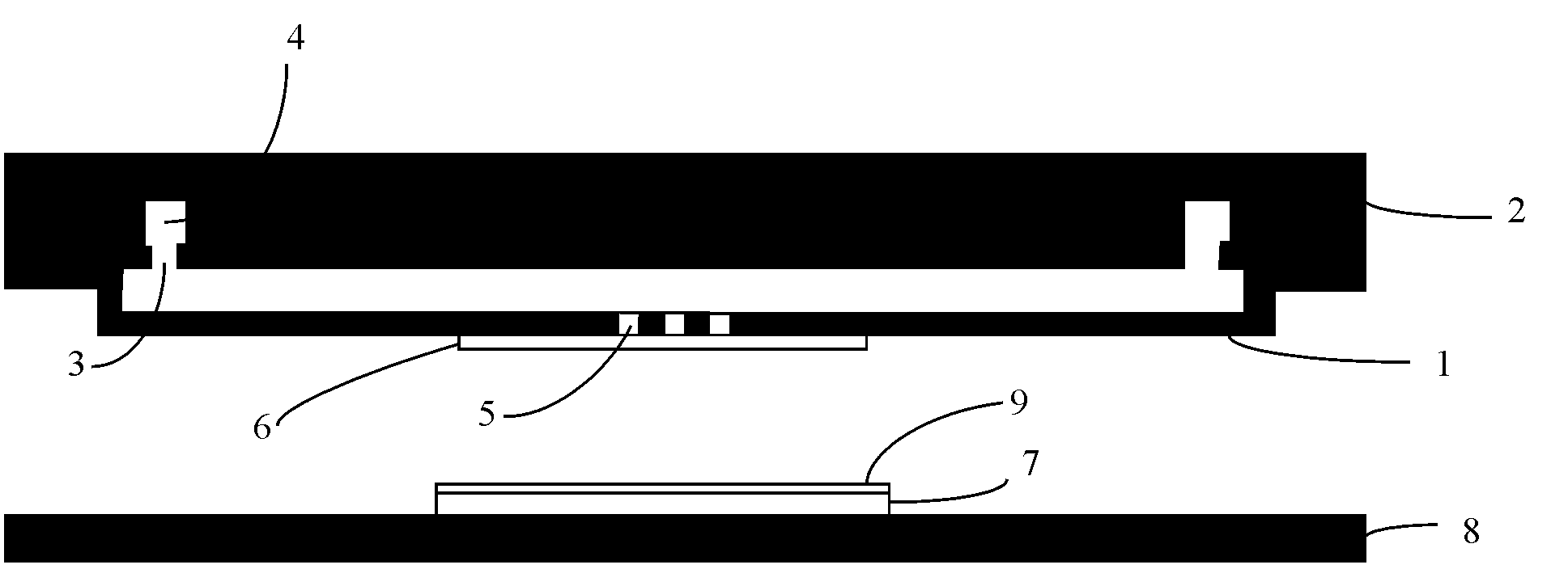
[0032] The invention adopts the nano-imprinting method combined with the nano-imprinting template fixing and aligning components to fix the nano-imprinting template and precisely align the nano-imprinting template and the graphic area of ​​the embossing substrate.

[0033] The present invention comprises the steps:

[0034] Step 1: Fix the stencil fixing and alignment component 1 with the stencil fixing jig 2 of the mask aligner, and the vacuum hole 3 on the upper part of the component 1 is located at the vacuum groove 4 of the stencil fixing jig 2 . After the vacuum is turned on, the vacuum suction passes through the vacuum groove 4 of the stencil fixing fixture 2, and is transmitted from the vacuum hole 3 in the component 1 to the vacuum hole 5 in the center of the lower surface of the component 1, and the stencil 6 is absorbed by the vacuum suction. At this position, the nanoimprint template 6 is fixed on the template fixing and alignment component 1 .

[0035] Step 2: Spi...


PUM


Abstract

The invention discloses a manufacturing method for micro-nano graphs used for an integrated optoelectronic device. The method comprises following steps: firstly, manufacturing an imprinting template and fixing the imprinting template and an imprinting substrate; secondly, aligning and attaching the imprinting template and the imprinting substrate, and imprinting the micro-nano graphs of the imprinting template on imprinting photoresist of the imprinting substrate; and finally, etching an integrated optoelectronic device micro-nano graph structure by taking the micro-nano graphs transferred to the imprinting photoresist as an etching mask. According to the invention, an aligning problem, during an integrated optoelectronic device manufacturing process, of a nano-imprinting method is solved, and the yield of nano-imprinted micro-nano graphs is greatly improved.

Description

technical field [0001] The invention relates to a method for manufacturing a micro-nano pattern for integrating optoelectronic devices, and belongs to the technical field of optoelectronics. Background technique [0002] With the development of optical communication, especially the ultra-high-speed and large-capacity requirements of optical communication systems, optoelectronic integration technology has become a hot field of scientific research. Optoelectronic integration adopts a manufacturing method similar to semiconductor integrated circuits to integrate optical components on the same substrate. This integrated device has the advantages of small size, long life, high reliability, low power consumption, and excellent performance. [0003] With the improvement of integration, the functions of devices are diversified, and the micro-nano pattern structure in integrated optoelectronic devices becomes more complex and the line width is smaller. Therefore, a stable and reliab...

Claims


Application Information

Patent Timeline
Patent Type & Authority Applications(China)
IPC IPC(8): G03F7/00G03F9/00
Inventor 余永林赵家霖唐怡超赵航
Owner HUAZHONG UNIV OF SCI & TECH
Why Eureka
Try Eureka