Manufacturing method of semiconductor device

A device manufacturing method and semiconductor technology, applied in the direction of semiconductor/solid-state device manufacturing, semiconductor devices, electrical components, etc., can solve the problems of reducing gate control capability and driving current, reducing the dielectric constant of high-K materials, and increasing EoT, etc., to achieve Improve gate control capability and drive current, optimize threshold voltage, and reduce the effect of EoT

Inactive Publication Date: 2014-03-12
INST OF MICROELECTRONICS CHINESE ACAD OF SCI
View PDF9 Cites 6 Cited by
  • Summary
  • Abstract
  • Description
  • Claims
  • Application Information

AI Technical Summary

Problems solved by technology

[0005] However, the above-mentioned traditional silicon oxide and then silicon nitride composite sidewalls will reduce the dielectric constant of high-K materials, increase EoT, and reduce gate control capability and drive current.

Method used


Image

  • Manufacturing method of semiconductor device
  • Manufacturing method of semiconductor device
  • Manufacturing method of semiconductor device

Examples


Embodiment Construction

[0029] The features and technical effects of the technical solution of the present invention will be described in detail below with reference to the accompanying drawings and in conjunction with exemplary embodiments. It should be pointed out that similar reference numerals indicate similar structures, and the terms "first", "second", "upper", "lower", "thick", "thin", etc. used in this application can be used for Modify various device structures. Unless otherwise specified, these modifications do not imply the spatial, order, or hierarchical relationship of the modified device structure.

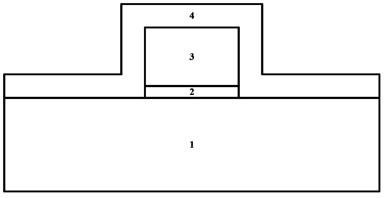
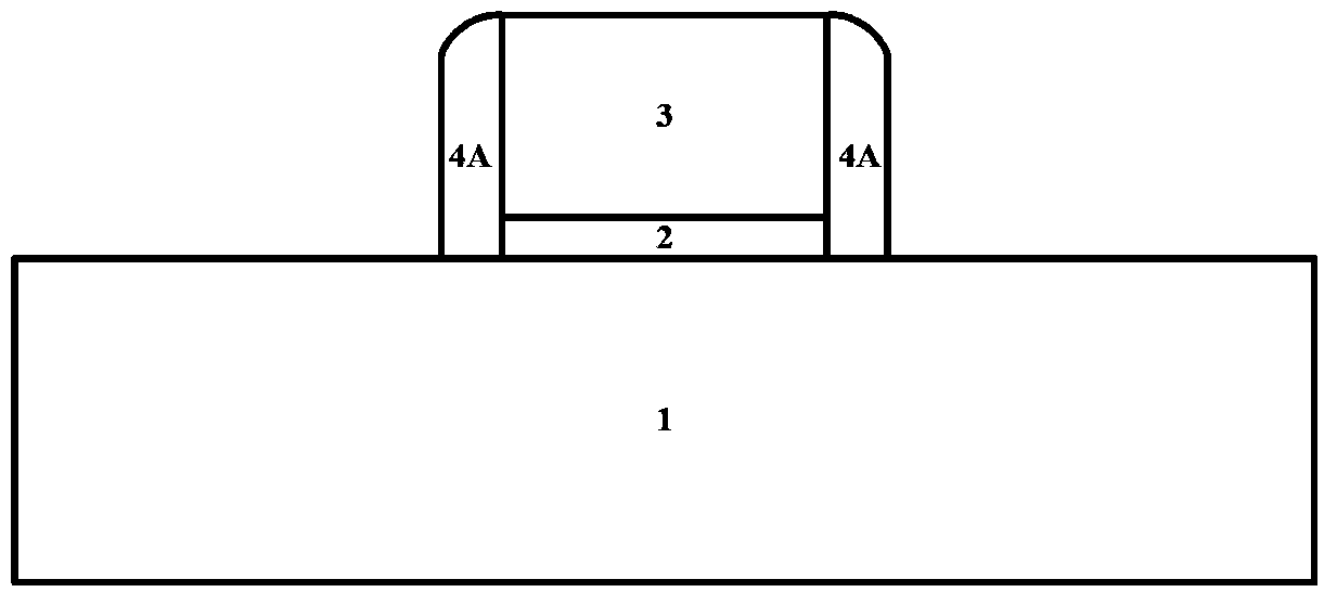
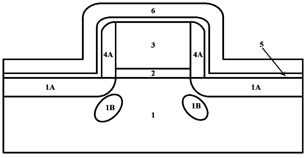
[0030] Reference Figure 5 as well as figure 1 , Forming a gate stack structure on the substrate, and depositing a first dielectric material layer on the substrate and the gate stack structure. The gate stack structure may be a gate stack of a front gate process or a dummy gate stack of a gate last process. A substrate 1 is provided, which may be bulk Si, SOI, bulk Ge, GeOI, SiGe, GeSb, or ...


PUM

PropertyMeasurementUnit
thicknessaaaaaaaaaa
thicknessaaaaaaaaaa

Abstract

Disclosed in the invention is a manufacturing method of a semiconductor device. The manufacturing method comprises the following steps: forming a grid stacking structure at a substrate; depositing a first dielectric material layer at the substrate and the grid stacking structure; etching the first dielectric material layer to form a first side wall; executing LDD and Halo doping injection; successively depositing a second dielectric material layer and a third dielectric material layer at the substrate and the first side wall; and successively etching the third dielectric material layer and the second dielectric material layer so as to form a third side wall and a second side wall respectively. According to the side wall etching method, the NON three-layer composite side wall is used and two-step etching is carries out, thereby reducing the damage on the substrate as well as the process complexity. Besides, the threshold voltage can be optimized; the EoT can be effectively reduced; and the grid-control capability and the drive current can also be improved.

Description

Technical field [0001] The present invention relates to the field of semiconductor integrated circuit manufacturing, and more specifically, to a sidewall etching method. Background technique [0002] In the manufacturing of very large scale integrated circuits, dielectric spacers need to be fabricated before the lightly doped drain (LDD) implantation process to prevent a larger dose of source and drain implants from being too close to the channel to cause the source and drain to pass through, resulting in device failure And the yield rate is reduced. [0003] Currently used in the mainstream 65nm or even 45nm sidewall manufacturing process: before the lightly doped drain (LDD) implantation process, first deposit or thermally grow a silicon dioxide thin film liner, such as rapid thermal oxidation (RTO) growth The silicon dioxide on the left and right is used as the subsequent etching stop layer to protect the substrate, especially the interface between the source and drain regions ...

Claims


Application Information

Patent Timeline
Patent Type & Authority Applications(China)
IPC IPC(8): H01L21/28H01L21/336
CPCH01L29/66492H01L29/42356
Inventor 孟令款
Owner INST OF MICROELECTRONICS CHINESE ACAD OF SCI
Why Eureka
Try Eureka