Formation of a layout structure for ultra-high withstand voltage resistors

A layout structure, high withstand voltage technology, applied in the direction of circuits, electrical components, electric solid devices, etc., can solve the problem of not being able to provide withstand voltage, and achieve the effect of solving insufficient withstand voltage

Active Publication Date: 2016-06-08
SHANGHAI HUAHONG GRACE SEMICON MFG CORP
View PDF5 Cites 0 Cited by
  • Summary
  • Abstract
  • Description
  • Claims
  • Application Information

AI Technical Summary

Problems solved by technology

However, when a high voltage is applied to the metal 305 at one end of the polysilicon and the metal 304 at the other end is grounded, since the silicon substrate 301 is connected to zero potential during chip operation, there is a high voltage difference between the polysilicon and the silicon substrate 301. The thickness of the field oxygen isolation between the polysilicon and the silicon substrate 301 is 4000A-6000A, so the polysilicon resistance can only withstand within 100V, and cannot provide higher withstand voltage applications

Method used


Image

  • Formation of a layout structure for ultra-high withstand voltage resistors
  • Formation of a layout structure for ultra-high withstand voltage resistors
  • Formation of a layout structure for ultra-high withstand voltage resistors

Examples


Embodiment Construction

[0017] The present invention will be further described in detail below in conjunction with the accompanying drawings and specific embodiments.

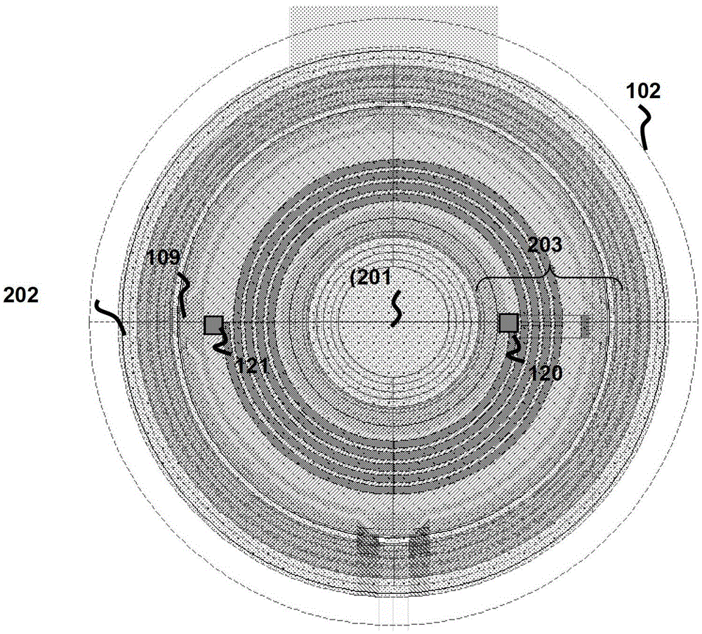
[0018] The layout structure for forming an ultra-high voltage resistance provided by the present invention takes an N-type high voltage field effect transistor as an example, including a circular N-type high voltage field effect transistor and a spiral polysilicon resistor;

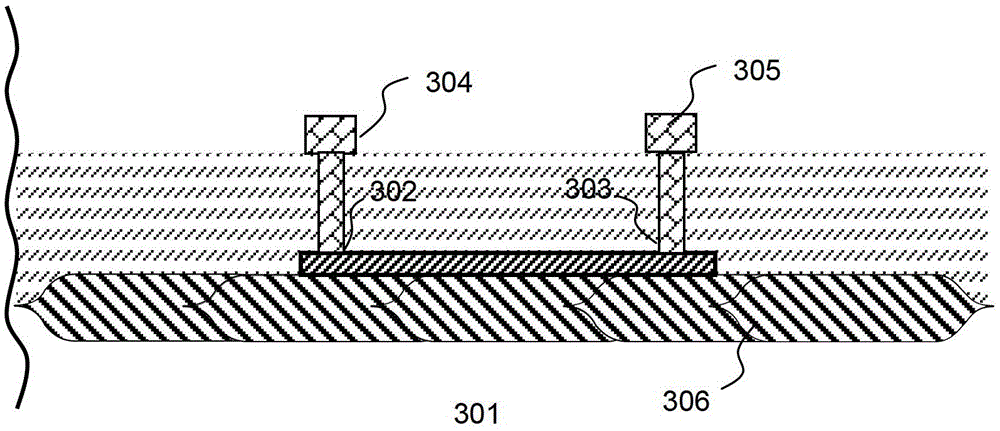
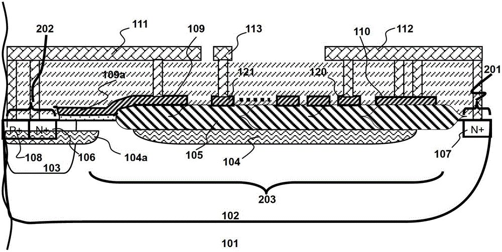
[0019] Such as figure 2 As shown, the N-type high withstand voltage field effect transistor includes a drain region 201, a source region 202, an N-type drain region drift region 203 and an N-type drift region 102; the N-type drift region 102 is located on a P-type silicon substrate 101, The drain region 201, the source region 202 and the N-type drain region drift region 203 are located in the N-type drift region 102; the drain region 201 is located in the center of the field effect transistor, and the N-type drain region drift region 102 is located between the d...


PUM


Abstract

The invention discloses a layout structure for forming an ultra-high withstand voltage resistance, which includes a high withstand voltage field effect transistor and a polysilicon resistor; the high withstand voltage field effect transistor includes a drain region, a source region, a drain region drift region and a drift region; the drain region Located in the center of the field effect transistor, the drain drift region is located between the drain region and the source region, and the source region is located outside the gate and surrounded by the drift region; field oxygen is formed in the drain region drift region, and the field oxygen is on the side near the drain region The polysilicon field plate in the drain region is formed, and the gate polysilicon is formed on the other side, and the gate polysilicon and the polysilicon field plate in the source region are connected laterally and connected to the source region; the polysilicon resistance is formed on the field oxygen and is located between the polysilicon field plate in the drain region and the gate polysilicon Between them, the high-voltage end is connected to the drain region of the high withstand voltage field effect transistor and the polysilicon field plate in the drain region through a metal wire, and the other end is led out through a metal wire. The invention utilizes the withstand voltage characteristics of the high withstand voltage field effect transistor to make the polysilicon resistance have the same withstand voltage capability as the high withstand voltage field effect transistor.

Description

technical field [0001] The invention relates to the field of semiconductor integrated circuits, in particular to a layout structure of ultra-high withstand voltage (greater than 300V) resistors. Background technique [0002] Currently used polysilicon resistors such as figure 1 As shown, the field oxide 306 is usually grown on the silicon substrate 301, and then polysilicon is grown on the field oxide 306, through holes 302, 303 are drilled at both ends of the polysilicon, and metals 304, 305 are drawn out respectively to form a resistance structure. As long as the resistance of this structure is large enough (for example, greater than 10MΩ), the current is small enough under high voltage (about 100V), and the polysilicon itself will not be damaged (generally, the polysilicon will be damaged if the current is greater than 20mA / μm). However, when a high voltage is applied to the metal 305 at one end of the polysilicon and the metal 304 at the other end is grounded, since the...

Claims


Application Information

Patent Timeline
Patent Type & Authority Patents(China)
IPC IPC(8): H01L27/02H01L29/78H01L29/40
CPCH01L29/42368H01L29/7816H01L29/405H01L29/063H01L29/1095
Inventor 金锋苗彬彬董金珠
Owner SHANGHAI HUAHONG GRACE SEMICON MFG CORP
Why Eureka
Try Eureka