In situ elliptical polarization measurement device

A technology of ellipsometry and measuring devices, which is applied in the directions of measuring devices, optical radiation measurement, and measuring the polarization of light. It can solve the problems of inconvenient operation, easily affecting the environment of the reaction chamber, and the inability to measure the thickness of the film, so as to keep clean and unobstructed, Ease of use

Active Publication Date: 2015-06-17
HUAZHONG UNIV OF SCI & TECH
View PDF4 Cites 0 Cited by
  • Summary
  • Abstract
  • Description
  • Claims
  • Application Information

AI Technical Summary

Problems solved by technology

[0006] The purpose of the present invention is to overcome the complex structure, inconvenient operation, inability to measure film thickness during a deposition cycle, and easy influence on the environment of the reaction chamber in the in-situ ellipsometry device with external pipes and isolation devices in the prior art. and other defects and deficiencies, an in-situ ellipsometric measurement device is provided, and an optical path hole for incident and reflection of polarized light is set on the sealing cover of the film reaction chamber, which can measure the thickness of the film at any time during the entire deposition process, and the cavity of the optical path hole The inner opening and the gas inlet and outlet of the reaction chamber are staggered, the gas flow in the reaction chamber is not easy to enter the optical path hole, so as to avoid the deposition of reactants on the inner wall of the optical path hole, and there is no need for complicated and regular cleaning. The structure of the whole measuring device is simple and compact. convenient

Method used


Image

  • In situ elliptical polarization measurement device
  • In situ elliptical polarization measurement device
  • In situ elliptical polarization measurement device

Examples


Embodiment Construction

[0020] In order to make the object, technical solution and advantages of the present invention clearer, the present invention will be further described in detail below in conjunction with the accompanying drawings and embodiments. It should be understood that the specific embodiments described here are only used to explain the present invention, not to limit the present invention.

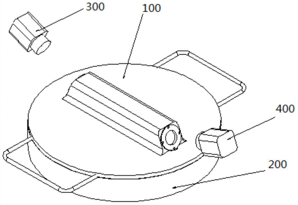
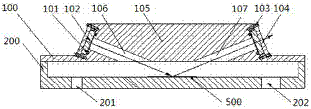
[0021] see figure 1 and figure 2 , the in-situ ellipsometry device provided by the present invention includes a sealing cover 100, a reaction chamber 200, a polarizer 300, an analyzer 400, and a deposition substrate 500. The upper surface of the sealing cover 100 is fixedly connected with a columnar boss 105, and The longitudinal axis of the boss 105 is parallel to the upper surface of the sealing cover 100 . The boss 105 is used to set the optical path hole for biasing. For the convenience of setting, the cross section of the boss 105 is preferably set to a rectangle or a trapezoid, and arc gui...


PUM


Abstract

An in situ elliptical polarization measurement device comprises a sealing cover (100); an incidence hole (106) and a reflection hole (107) which respectively allow incidence and reflection of a polarized light are arranged on the sealing cover; an incidence light penetration mouth (108) and a reflection light penetration mouth (109) which are sealed are respectively arranged at outer openings of the incidence hole and the reflection hole; while a thin film reaction cavity is maintained closed, a thin film thickness can be measured at any moment in an atomic layer deposition process; an opening within a cavity of an optical path hole, and air inlet and outlet mouths of a reaction cavity are staggered, so that an air flow in the reaction cavity is not easy to enter the optical path hole and a reagent is prevented from depositing on an inner wall of the optical path hole; the complex regular cleaning is not needed; and the whole measuring device is simple and compact in structure, and easy to use.

Description

technical field [0001] The invention relates to a device and a measuring method for measuring the thickness of an atomic layer deposition film, in particular to a device for measuring the thickness of an atomic layer deposition film in situ by an ellipsometer. Background technique [0002] With the continuous development of semiconductor integrated circuits, the chip size is continuously reduced and the performance is continuously improved, and there is an urgent need for thin films with high precision and nanometer thickness. Atomic layer deposition technology has gradually replaced the traditional chemical vapor deposition and physical vapor deposition methods due to its nano-controllable film thickness and good uniformity, and is widely used in micro-nano electronic devices, solar cells and other fields. The technical principle of atomic layer deposition is that a precursor is introduced into a vacuum chamber and chemically adsorbed on the surface of the substrate (usuall...

Claims


Application Information

Patent Timeline
Patent Type & Authority Patents(China)
IPC IPC(8): G01J4/00G01B11/06
Inventor 陈蓉何文杰曹坤周雪琪单斌文艳伟
Owner HUAZHONG UNIV OF SCI & TECH
Why Eureka
Try Eureka