Supercharge Your Innovation With Domain-Expert AI Agents!

Transistor threshold-voltage testing circuit

A technology for testing circuits and threshold voltages. It is applied in the direction of single semiconductor device testing, measuring current/voltage, and measuring devices. It can solve the problems of not being able to measure threshold voltages, achieve accurate evaluation and testing, and improve accuracy.

Active Publication Date: 2014-03-26
SEMICON MFG INT (SHANGHAI) CORP
View PDF7 Cites 3 Cited by
  • Summary
  • Abstract
  • Description
  • Claims
  • Application Information

AI Technical Summary

Problems solved by technology

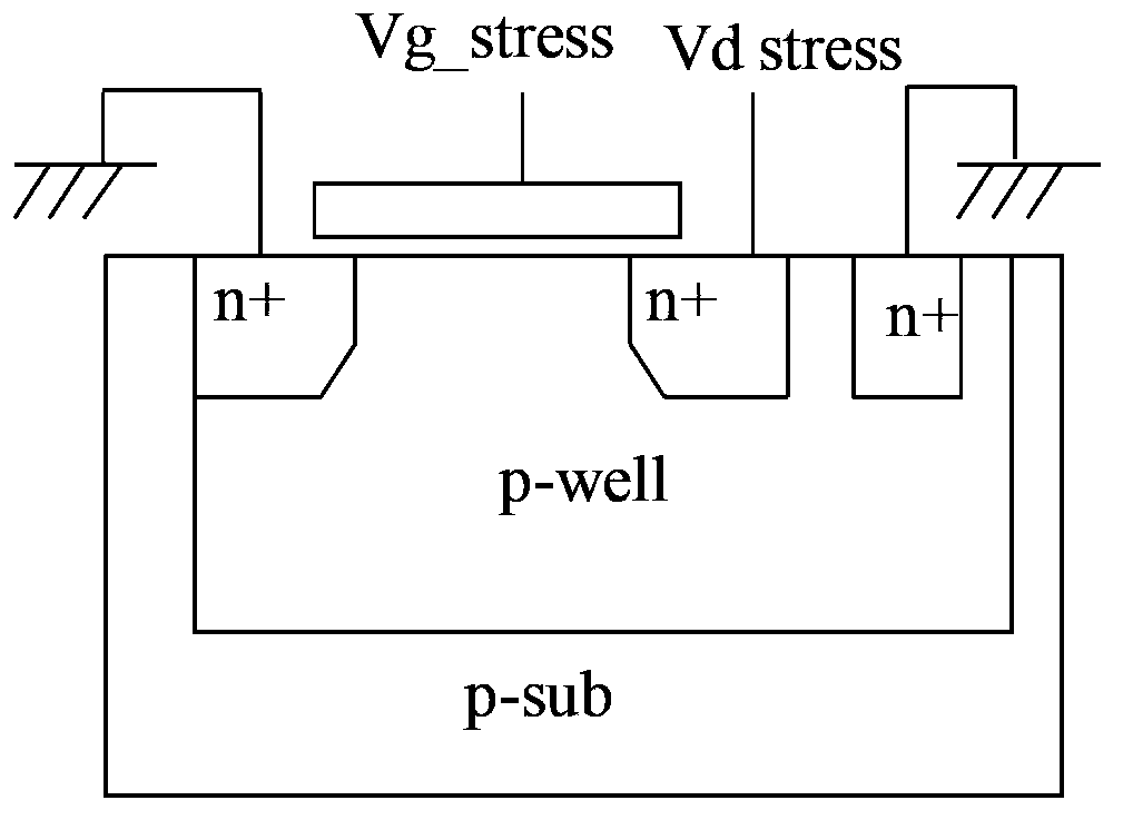
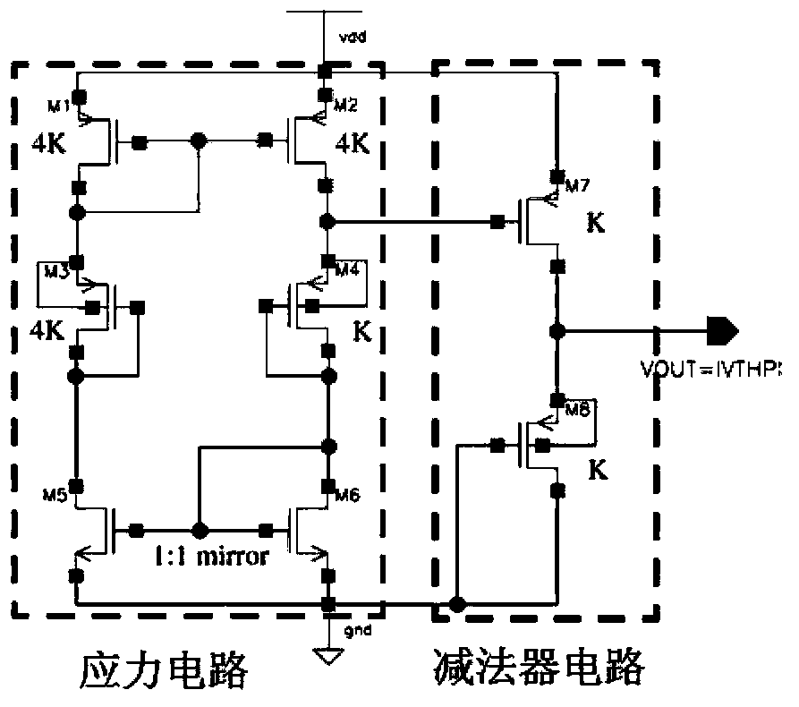
[0003] In order to be able to account for the impact of HCI, there is an urgent need to provide a test structure that can detect both factors of threshold voltage (Vth) and saturation drain current (Idsat) drift, the test structure can not only characterize both but also It is possible to analyze the impact of these two effects on the circuit. At present, the device-level bias gate voltage detection device in the prior art is as follows: figure 1 As shown, after the source drain and the substrate are grounded, then the gate voltage is applied to the gate, and the drain voltage is applied to the drain, the bias occurs. The extraction circuit of the threshold voltage (Vth) is as follows figure 2 As shown, the shown circuit includes 8 MOSFETs, M1-M8, one end of the NMOS and PMOS is grounded, and the operating voltage of the chip is applied, and a pair of mirror current circuits are formed by transistors M1, M2, M5, and M6. connected to form a closed current feedback loop, thus obtaining the V of M1 Out , the V Out equal to the threshold voltage (Vth) of transistor M1, but the currents in the circuit are forced to track and match each other, and the test circuit is not applicable for measuring threshold voltage (Vth) and saturation drain current (Idsat) drift Therefore, in order to better evaluate and test the HCI effect, the above problems must be solved

Method used


Image

  • Transistor threshold-voltage testing circuit
  • Transistor threshold-voltage testing circuit
  • Transistor threshold-voltage testing circuit

Examples


Embodiment Construction

[0028] In the following description, numerous specific details are given in order to provide a more thorough understanding of the present invention. It will be apparent, however, to one skilled in the art that the present invention may be practiced without one or more of these details. In other examples, some technical features known in the art are not described in order to avoid confusion with the present invention.

[0029] It should be noted that the terms used herein are for the purpose of describing specific embodiments only, and are not intended to limit exemplary embodiments according to the present invention. As used herein, singular forms are intended to include plural forms unless the context clearly dictates otherwise. In addition, it should also be understood that when the terms "comprising" and / or "comprising" are used in this specification, it indicates the presence of the features, integers, steps, operations, elements and / or components, but does not exclude th...


PUM


Abstract

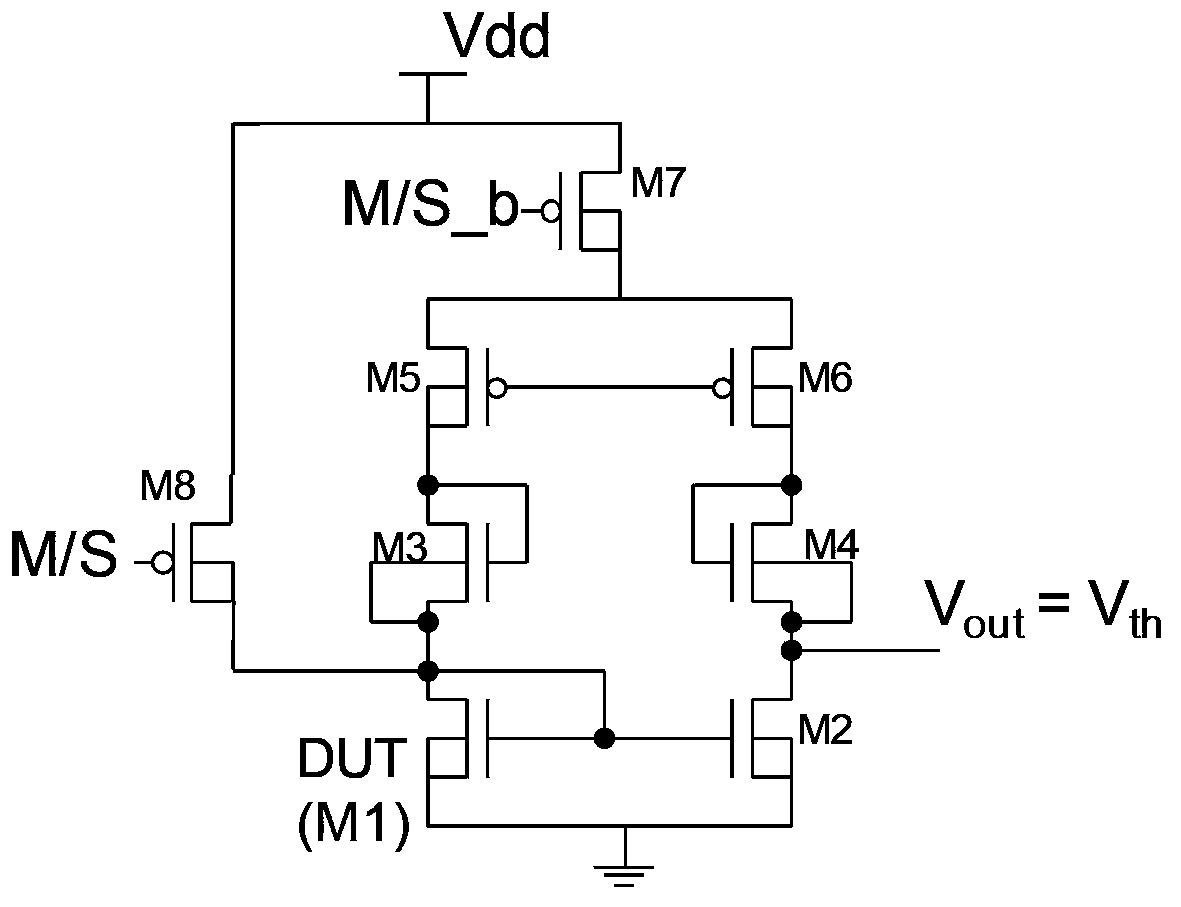
The invention relates to a transistor threshold-voltage testing circuit which includes a threshold-voltage stress circuit. The threshold-voltage stress circuit includes an image-current circuit which includes a transistor to be tested. One end of the image-current circuit is connected with a power supply and the other end is grounded. The transistor threshold-voltage testing circuit is characterized by also including a switching circuit which includes a first transistor and a second transistor. The first transistor is arranged between the power supply and the transistor to be tested. A grid electrode of the first transistor is connected with a first measurement control signal. The second transistor is arranged between the power supply and the image-current circuit. A grid electrode of the second transistor is connected with a second measurement control signal. The switching circuit controls the threshold-voltage stress circuit to be in a stress state and a measurement state respectively. Thorough the two states, the threshold voltage of the transistor to be tested is measured.

Description

technical field [0001] The invention relates to the field of semiconductors, and in particular, the invention relates to a test circuit for transistor threshold voltage. Background technique [0002] For the VLSI manufacturing industry, with the continuous reduction in the size of MOSFET (Metal Oxide Semiconductor Field Effect Transistor) devices, the semiconductor manufacturing process has entered the era of deep submicron, and is developing towards ultra-deep submicron. At this time, The reliability of semiconductor devices directly affects the performance and service life of IC chips produced. However, when the size of the MOS device is reduced proportionally, the operating voltage of the device does not decrease correspondingly, so the electric field strength inside the corresponding device increases with the reduction of the device size. Therefore, in small-sized devices, the lateral size of the circuit is getting smaller and smaller, resulting in a decrease in the cha...

Claims


Application Information

Patent Timeline
IPC IPC(8): G01R31/26G01R19/00
Inventor 甘正浩冯军宏
Owner SEMICON MFG INT (SHANGHAI) CORP
Features
  • R&D
  • Intellectual Property
  • Life Sciences
  • Materials
  • Tech Scout
  • Unparalleled Data Quality
  • Higher Quality Content
  • 60% Fewer Hallucinations
Learn More