A real time on-line test system for MOS chip gamma ray radiation responses

A radiation response, online testing technology, applied in the field of radiation detection, can solve the problems of imperfect testing system and inaccurate results, and achieve the effect of reducing manual debugging time and errors, safe experimental environment, and accurate debugging

Inactive Publication Date: 2014-03-26
XIAN JIAOTONG LIVERPOOL UNIV
View PDF7 Cites 11 Cited by
  • Summary
  • Abstract
  • Description
  • Claims
  • Application Information

AI Technical Summary

Problems solved by technology

[0007] The purpose of the present invention is to provide a real-time online test system for MOS chip gamma ray radiation response, which solves the problem of lack of corresponding MOS chip gamma ray radiation response detection in the prior art, which is manual testing, imperfect test system, and test due to chip radiation degradation. lead to inaccurate results

Method used


Image

  • A real time on-line test system for MOS chip gamma ray radiation responses
  • A real time on-line test system for MOS chip gamma ray radiation responses
  • A real time on-line test system for MOS chip gamma ray radiation responses

Examples


Embodiment

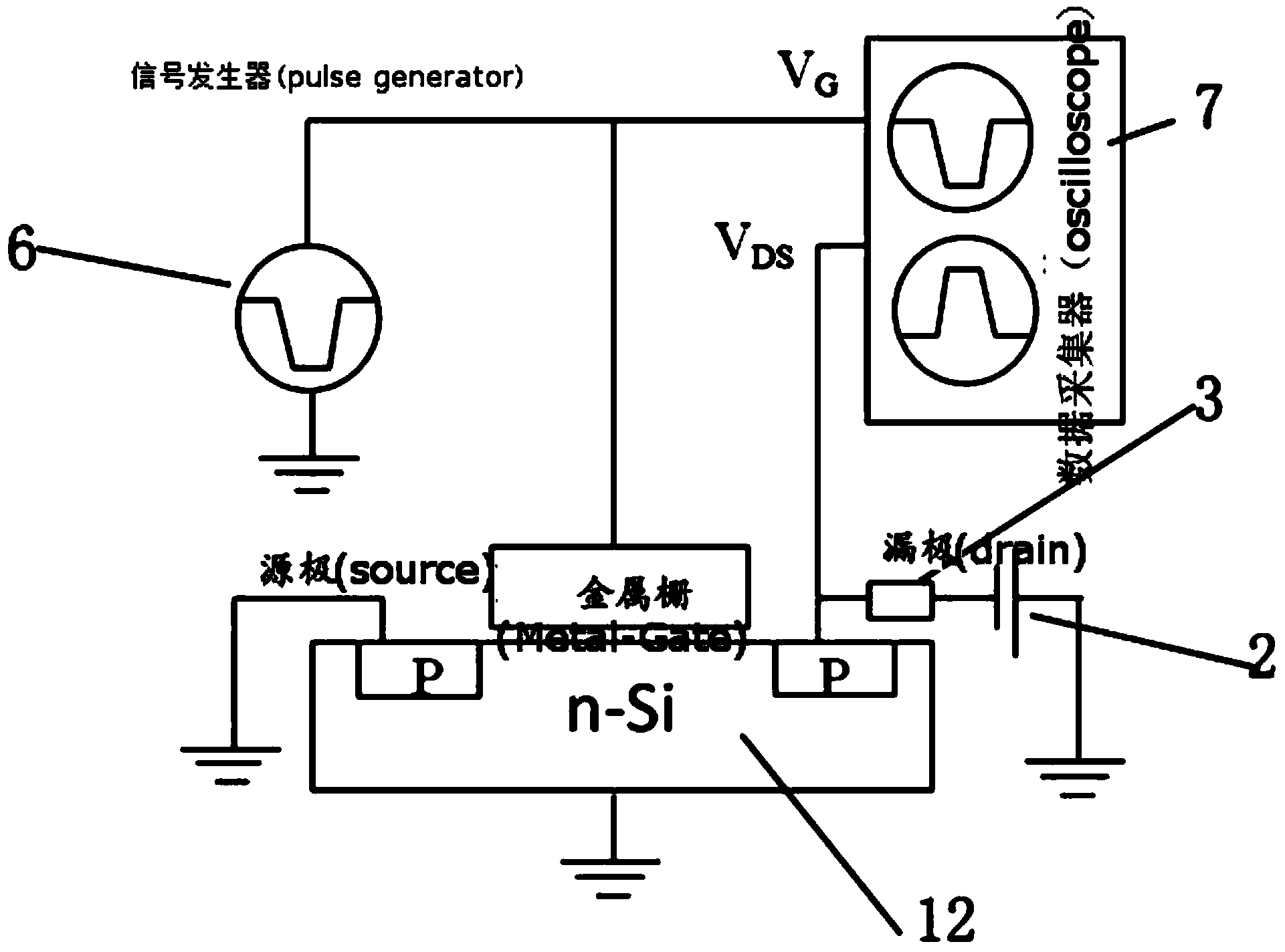
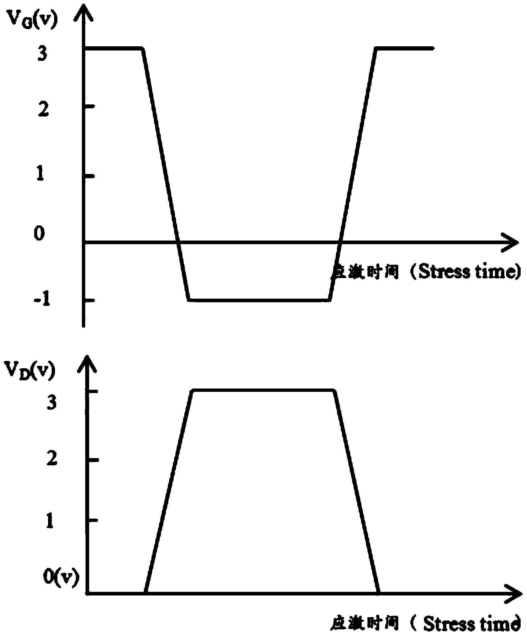
[0058] Such as Figure 1 to Figure 6 As shown, the real-time online test system that can be used for MOS chip gamma-ray radiation response includes radiation response probe station 1, Figure 5 The pulsed I-V test system shown, Figure 6 The pulsed C-V test system shown and Figure 4 On-The-Fly test system shown.

[0059] The radiation response probe station 1 includes a radioactive source 10 placed in a lead container, the chip to be tested 12 is placed at the upper opening of the lead container, the chip to be tested 12 is connected to a probe 14, and the probe 14 Connects to Pulse I-V Test System, Pulse C-V Test System and On-The-Fly Test System. The lead container includes a cover cylinder 111 and a lead base 112. The upper end of the cover cylinder 111 is placed in the lead protective layer 15, and the lower end is placed on the lead container base 9 whose position can be adjusted remotely. The upper side of the lead container is surrounded by a lead protective layer ...


PUM


Abstract

The invention discloses a real time on-line test system for MOS chip gamma ray radiation responses. The real time on-line test system is characterized in that: the system comprises a radiation response probe bench (1), a pulse I-V test system, a pulse C-V test system and an On-The-Fly test system. The radiation response probe bench (1) comprises a lead container with a built-in radioactive source (10), a to-be-tested chip (12) and a microscope (13) observing changes of the to-be-tested chip. The lead container has an opening at the upper end. The to-be-tested chip (12) is placed in the opening portion of the lead container. The upper end of the to-be-tested chip (12) is connected with a probe (14). The probe is separately connected with the pulse I-V test system, the pulse C-V test system and the On-The-Fly test system. The system fills a technical gap of real time on-line monitoring for the MOS chip gamma ray radiation responses, and a basis is provided for the development application of radiation-proof integrated circuits and high-K medium radiation responses.

Description

technical field [0001] The invention belongs to the technical field of radiation detection, in particular to a real-time on-line test system for gamma ray radiation response of a MOS chip. Background technique [0002] With the development of space technology and the wide application of nuclear industry, nuclear power plants and radioactive medical devices in daily life, the impact of ionizing radiation on various electronic devices cannot be ignored. Therefore, the reliability of semiconductor devices in these electronic devices in radiation environments Sexuality studies have become very important. [0003] The general semiconductor material ionizing radiation damage test uses the "over-radiation" method, that is, after the semiconductor device is irradiated, the radiation damage is measured and analyzed. However, after a period of time, the damage caused by ionizing radiation to semiconductor materials will be significantly degraded. In addition, the traditional I-V and ...

Claims


Application Information

Patent Timeline
Patent Type & Authority Applications(China)
IPC IPC(8): G01R31/28
Inventor 慕轶非赵策洲
Owner XIAN JIAOTONG LIVERPOOL UNIV
Why Eureka
Try Eureka