Silicon substrate air-impermeability sealing structure and manufacturing method thereof

A sealing structure and air-tight technology, which is applied in semiconductor/solid-state device manufacturing, electrical components, electric solid-state devices, etc., can solve the problems of poor structural strength, large pitch between through holes, and large package size, etc., to achieve reduced package size Size, simplify the production process, improve the effect of structural strength

Active Publication Date: 2014-03-26
58TH RES INST OF CETC
View PDF4 Cites 10 Cited by
  • Summary
  • Abstract
  • Description
  • Claims
  • Application Information

AI Technical Summary

Problems solved by technology

Moreover, due to the thin thickness of this type of silicon substrate and the large pitch between vias, the practical application of TSV technology is limited, resulting in large package size and poor st

Method used


Image

  • Silicon substrate air-impermeability sealing structure and manufacturing method thereof
  • Silicon substrate air-impermeability sealing structure and manufacturing method thereof
  • Silicon substrate air-impermeability sealing structure and manufacturing method thereof

Examples


Embodiment Construction

[0023] The present invention will be further described below in conjunction with drawings and embodiments.

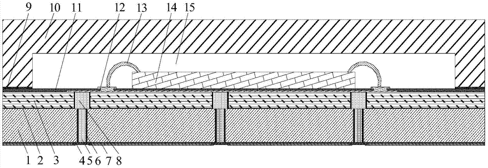
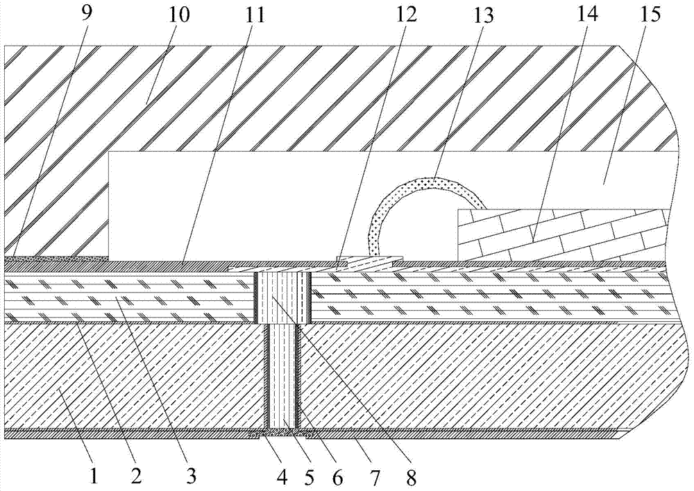
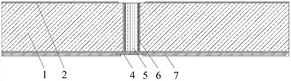
[0024] Such as figure 1 , as shown in 2, the silicon-based hermetic sealing structure of the present invention comprises a silicon substrate 1, a through hole is made on the silicon substrate 1, a first insulating layer 2 is deposited on the surface of the silicon substrate 1, and a seed layer is deposited on the inner wall of the through hole Metal 6, and then fill the first metal 5 in the through hole, the first metal wiring layer 4 is deposited on the back of the first metal 5; the front of the silicon substrate 1 is filled with a polymer dielectric layer 3, and the polymer dielectric layer 3 corresponds to Each position filled with the first metal 5 is made with an opening, and the opening is filled with the second metal 8; the upper surface of the polymer dielectric layer 3 is provided with a second metal wiring layer 12 and a second insulating layer 11, and the se...


PUM


Abstract

The invention discloses a silicon substrate air-impermeability sealing structure and a manufacturing method thereof. The sealing structure comprises a silicon substrate provided with a complete through hole filled with first metal, the surface of the silicon substrate is passivated, and the back face of the silicon substrate is provided with a bonding pad. The front face of the silicon substrate is filled with a polymer dielectric layer provided with an opening which is filled with second metal. The upper surface of the polymer dielectric layer is provided with a metal wiring layer and an insulating layer. The second metal wiring layer and the second metal are in contact to form electric connection. A chip is mounted on the upper surface of a second insulating layer. A pin of the chip is electrically connected with the second metal wiring layer through a bonding wire, and the second metal wiring layer and the second metal are in direct contact to form electric connection. The second metal and the first metal are in direct contact to form electric connection. A cover plate and the silicon substrate are sealed together through sealing materials to form a cavity. The silicon substrate air-impermeability sealing structure and the manufacturing method thereof can effectively reduce the packaging size, improve structural strength, and simplify the production technology.

Description

technical field [0001] The invention relates to a silicon-based airtight sealing structure and a manufacturing method thereof, belonging to the technical field of integrated circuit packaging. Background technique [0002] Through-silicon via technology (TSV) is currently the main development direction of integrated circuits. Because of its excellent high-frequency characteristics, it can reduce transmission delay, reduce noise, small package size, and high thermal expansion reliability. Also wider. [0003] Through-silicon via technology (TSV) is limited by equipment capabilities, especially the sidewall insulating layer and barrier layer sputtering of high-aspect-ratio through-holes is quite difficult. For this reason, the industry usually makes the silicon substrate relatively thin for later The through-hole filling process; and for the sake of structural strength, the pitch of the through-holes is generally set larger. Moreover, due to the thin thickness of this type o...

Claims


Application Information

Patent Timeline
IPC IPC(8): H01L23/538H01L23/02H01L21/768H01L21/60H01L21/50
CPCH01L2224/48091
Inventor 吉勇燕英强丁荣峥李欣燕
Owner 58TH RES INST OF CETC
Why Eureka
Try Eureka