Double-bit flash memory, and manufacturing method and operation method thereof

A dual-bit, flash memory technology, applied in the field of dual-bit flash memory, the manufacture of dual-bit flash memory, and the operation of dual-bit flash memory, can solve the problems of data reliability, small distance, and easy interference of storage units.

Active Publication Date: 2014-03-26
SHANGHAI HUAHONG GRACE SEMICON MFG CORP
View PDF3 Cites 15 Cited by
  • Summary
  • Abstract
  • Description
  • Claims
  • Application Information

AI Technical Summary

Problems solved by technology

However, a shortcoming of the cell structure of the existing double-bit flash memory is that the distance between the ONO layer 203 and the

Method used


Image

  • Double-bit flash memory, and manufacturing method and operation method thereof
  • Double-bit flash memory, and manufacturing method and operation method thereof
  • Double-bit flash memory, and manufacturing method and operation method thereof

Examples


Embodiment Construction

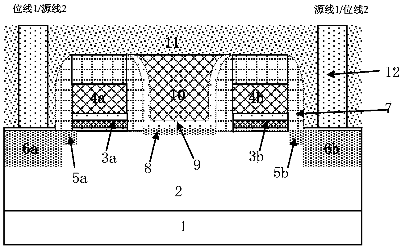
[0051] Such as image 3 Shown is a schematic diagram of the cell structure of the dual-bit flash memory in the embodiment of the present invention; the cell structure of the dual-bit flash memory in the embodiment of the present invention includes: a first SONOS memory, a second SONOS memory, and a selection tube.

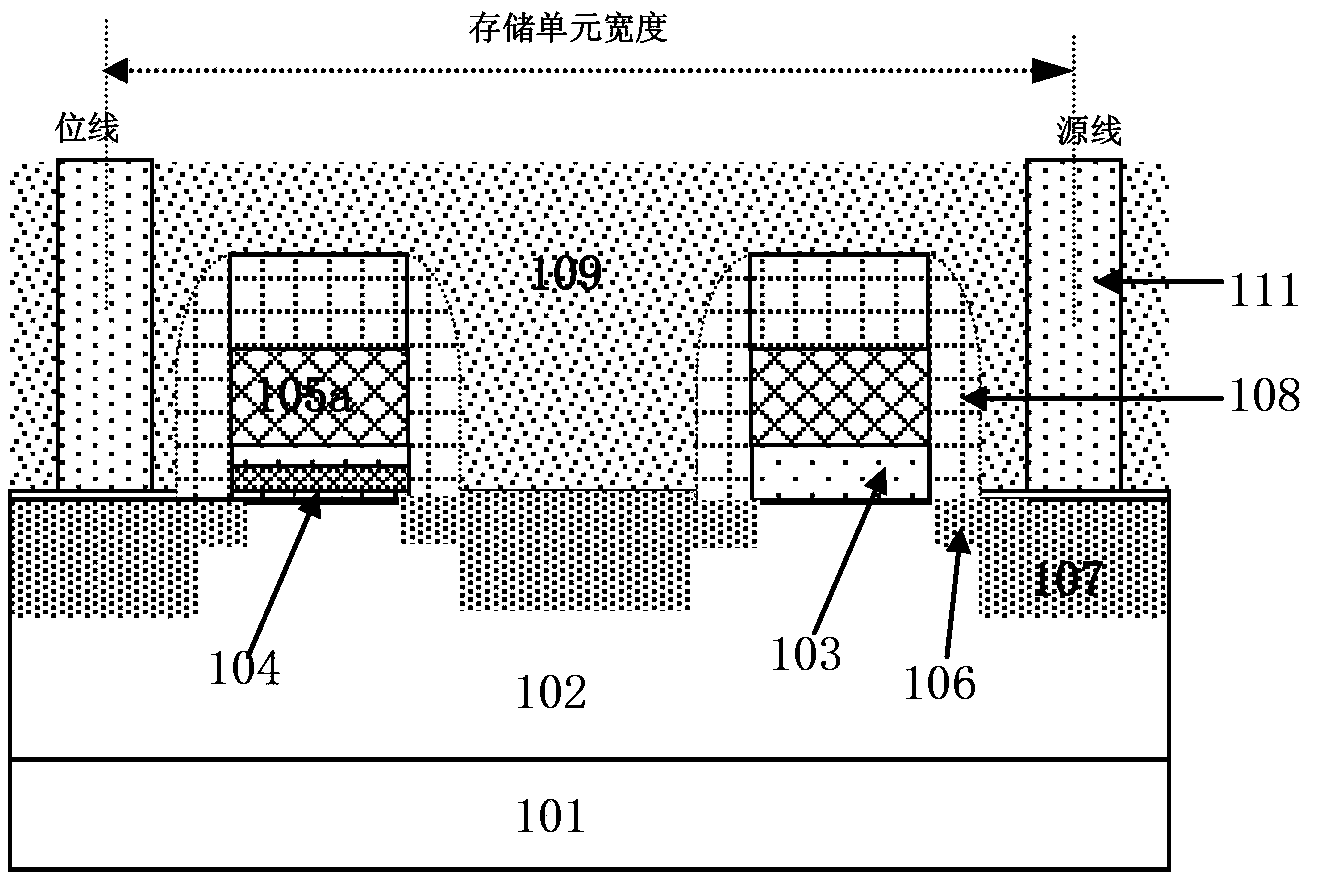
[0052] The substrate structure used in the cell structure of the dual-bit flash memory in the embodiment of the present invention is a semiconductor substrate such as a silicon substrate. A deep N-well 1 is formed on the silicon substrate and defined by shallow trench isolation on the silicon substrate. An active region is formed. A P well 2 is formed in the active region of the cell structure region of the dual-bit flash memory in the embodiment of the present invention, and the P well 2 is located on the deep N well 1.

[0053] The gate structure of the first SONOS memory includes an ONO layer 3a composed of a first oxide layer, a second nitride layer, and a third oxid...


PUM


Abstract

The invention discloses a double-bit flash memory which includes two adjacent SONOS memories which are in the same active region and a selection pipe located between the two SONOS memories. The position and size of a gate structure of the selection pipe are directly defined by self alignment of two adjacent side walls between the two SONOS memories. The invention also discloses a manufacturing method for the double-bit flash memory. The invention also discloses an operation method for a double-bit flash memory. The double-bit flash memory is capable of realizing storage of two-digit data in a single unit structure so that not only is storage density improved and device area reduced, but interferences between the two-digit data are also prevented and thus the reliability of the data is improved.

Description

Technical field [0001] The invention relates to the field of semiconductor integrated circuit manufacturing, in particular to a dual-bit flash memory; the invention also relates to a method for manufacturing the dual-bit flash memory; the invention also relates to an operating method of the dual-bit flash memory. Background technique [0002] Embedded non-volatile memory (NVM) technology has developed so far, mainly including floating gate technology, split gate technology, and SONOS (Silicon-Oxide-Nitride-Oxide-Silicon). Silicon) technology. Floating gate NVM has the advantage of higher data retention capability compared to other technologies, but it faces difficulties in size reduction. SONOS technology is widely used and has the advantages of low operating voltage, fast speed, and large capacity. With the rapid development of mobile Internet technology, especially the rapid rise of the semiconductor market with mobile terminals as the main market application, the emerging se...

Claims


Application Information

Patent Timeline
IPC IPC(8): H01L27/115H01L21/8247G11C16/06
Inventor 陈广龙谭颖杨志王喆张可刚陈华伦
Owner SHANGHAI HUAHONG GRACE SEMICON MFG CORP
Why Eureka
Try Eureka