Two-stage time-to-digital converter

A time-to-digital converter technology, applied in the field of two-stage time-to-digital converters, can solve the problems of time quantization complexity and achieve the effect of easy matching, high resolution and linearity

Inactive Publication Date: 2014-03-26
FUDAN UNIV
View PDF2 Cites 21 Cited by
  • Summary
  • Abstract
  • Description
  • Claims
  • Application Information

AI Technical Summary

Problems solved by technology

[0005] At present, the difficulty of the two-stage TDC applied to the high-frequency broadband ADPLL is that the high-frequency broadband sig

Method used


Image

  • Two-stage time-to-digital converter
  • Two-stage time-to-digital converter
  • Two-stage time-to-digital converter

Examples


Embodiment 1

[0033] The TDC designed in this example is a TDC used in a 1.2G-2.5GHz all-digital phase-locked loop (ADPLL). Its reference frequency is 40MHz. (The highest sampling ratio) is 2.5G / 40M=62.5, the highest and lowest frequency ratio>2, which can be called broadband.

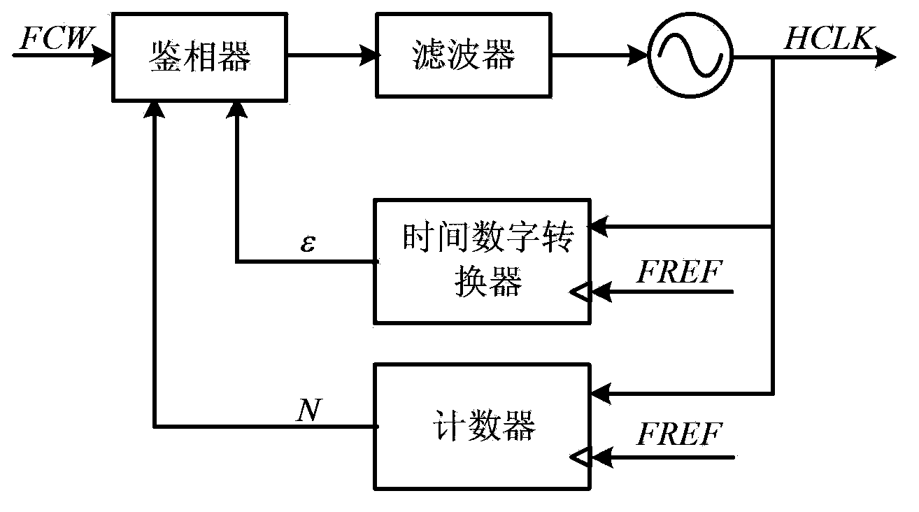
[0034] The structure of the all-digital phase-locked loop (ADPLL) applicable to the two-stage TDC proposed in this example is as follows: figure 1 As shown, the role of TDC in it is to quantify the time interval between HCLK and FREF, and at the same time normalize the period of HCLK, and finally obtain the fractional frequency division ratio and input it to the following circuit.

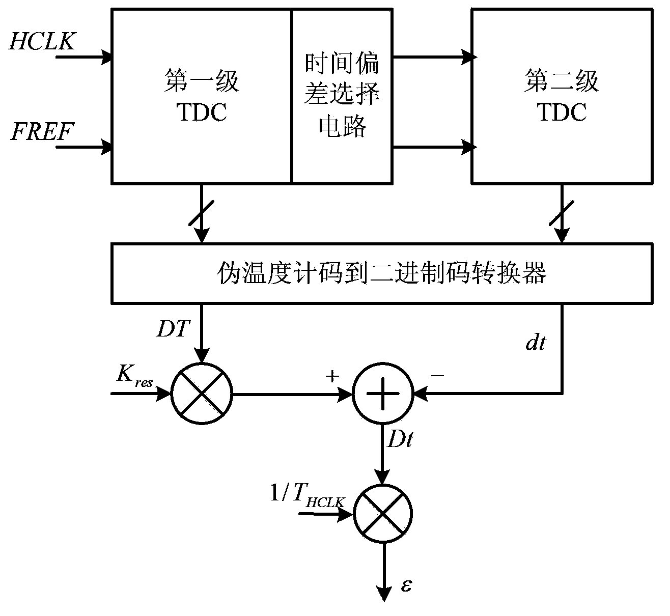
[0035] The TDC frame structure proposed in this example is as follows: figure 2 As shown, it includes a two-stage quantization circuit and a decoding circuit. The first-stage quantization is coarse quantization, the second-stage quantization is fine quantization, and the deviation selection circuit is between the two-stage quantization...


PUM


Abstract

The invention belongs to the field of microelectronics and time measurement, and particularly relates to a two-stage time-to-digital converter. The circuits of the converter can be applied to all digital phase-locked loops (ADPLL) with high frequency wide bands. According to the two-stage time-to-digital converter of the invention, the combination of semi custom and full custom is adopted, and two-stage time-to-digital converter comprises a first-stage quantizing structure, a time deviation selection circuit, a second-stage quantizing structure and a decoding circuit, wherein the first-stage quantizing structure adopts a buffer delay chain for coarse quantization; the time deviation selection circuit is composed of a selective signal generator, a delay chain and a multiplexer; the second-stage quantizing structure adopts a Vernier delay chain using a buffer as a basic unit to carry out fine quantization, and a duplication chain comprising a first-stage buffer chain simultaneously multiplexes the Vernier delay chain for measurement of a resolution ratio; the decoding circuit corresponds to a quantization scheme to realize transformation from pseudo thermometer codes to binary codes; the selective signal generator and the decoding circuit are realized by Verilog semi-custom, and the rest are realized by full-custom. The two-stage time-to-digital converter of the invention can be applied to ADPLL with the high frequency wide bands so as to realize time-to-digital conversion with high resolution and linearity.

Description

technical field [0001] The invention belongs to the field of microelectronics and time measurement, and in particular relates to a two-stage time-to-digital converter. The circuit of the converter can be applied to a high-frequency and wide-band all-digital phase-locked loop. Background technique [0002] With the advancement of process reduction, a time-to-digital converter (Time to Digital Converter, TDC) can achieve higher and higher resolutions. The prior art discloses that the time-to-digital converter TDC is the key to the digitization of a phase-locked loop (PLL, Phase Lock Loop). Generally, digital PLL (DPLL, Digital PLL) includes counter-assisted all-digital phase-locked loop (ADPLL, All Digital PLL) and frequency divider-assisted DPLL, the latter is hindered by high-frequency limitations and the complexity of frequency divider design Full digital implementation. [0003] According to research reports, the TDC used in the counter-assisted ADPLL is to measure the i...

Claims


Application Information

Patent Timeline
IPC IPC(8): H03M1/50
Inventor 李巍纪伟伟
Owner FUDAN UNIV
Why Eureka
Try Eureka