Electrostatic vapor deposition method and device for OEL (organic electroluminescence) display materials

An electroluminescence display and luminescence technology, which is applied in the direction of vacuum evaporation plating, metal material coating process, circuit, etc., can solve the problems of not being able to be used, deformed, and affecting the shape accuracy of the pattern formed by evaporation, so as to achieve the goal of evaporation deposition The effect of high accuracy of position and shape

Inactive Publication Date: 2014-04-02
BOE TECH GRP CO LTD
View PDF4 Cites 20 Cited by
  • Summary
  • Abstract
  • Description
  • Claims
  • Application Information

AI Technical Summary

Problems solved by technology

[0005] However, the existing electrostatic evaporation methods for OEL materials have the following problems: First, due to the thermal stress generated by gravity and temperature changes, deformation will occur, which affects the position and pattern shape accuracy of evaporation formation; second, due to the FMM shielding effect, only a small amount OEL materials are deposited on the light-emitting layer through FMM, and the rest of the materials cannot be used because they are deposited on FMM

Method used


Image

  • Electrostatic vapor deposition method and device for OEL (organic electroluminescence) display materials
  • Electrostatic vapor deposition method and device for OEL (organic electroluminescence) display materials
  • Electrostatic vapor deposition method and device for OEL (organic electroluminescence) display materials

Examples


Embodiment approach

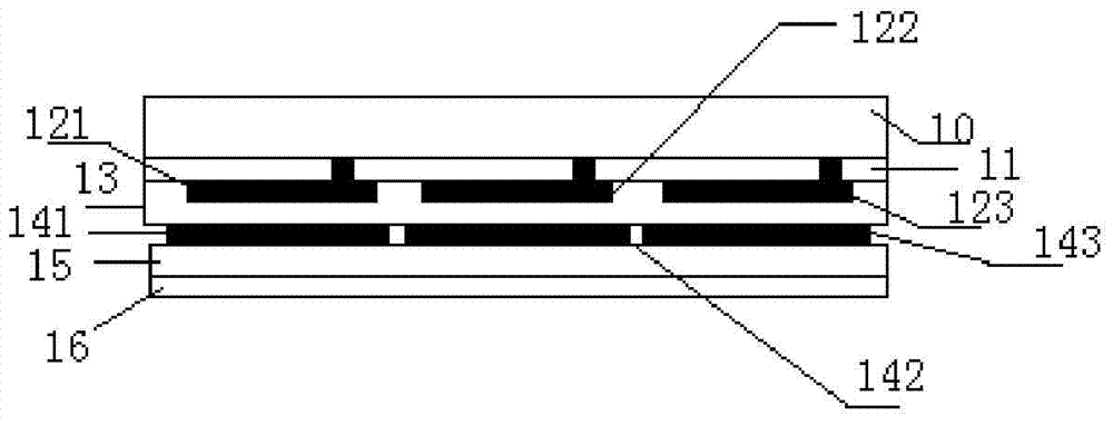
[0054] According to a specific embodiment, when the red light emitting layer, the green light emitting layer and the blue light emitting layer need to be evaporated sequentially,

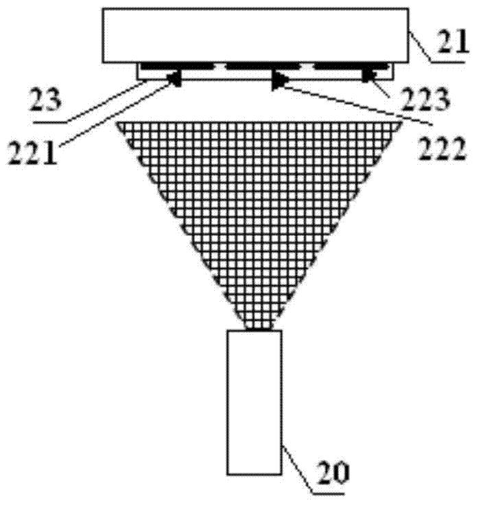
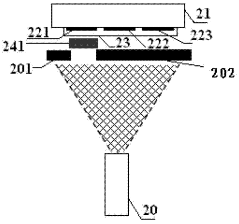
[0055] like Figure 4A As shown, first, the OEL material evaporation source 40 performs evaporation of the light-emitting layer lower structure 43 on the OLED display backplane 42 provided with the red sub-pixel electrode 411, the green sub-pixel electrode 412 and the blue sub-pixel electrode 413;

[0056] like Figure 4B As shown, the evaporation of the red light-emitting layer is carried out again: the OEL material evaporation source 40 outputs red OEL material particles;

[0057] Particle Charging and Transport Module ( Figure 4B not shown in the figure) to control the red OEL material particles to be positively charged, and make the positively charged red OEL material particles directional transport or scatter toward the OLED display backplane 42;

[0058] Particle speed control module (incl...


PUM


Abstract

The invention provides an electrostatic vapor deposition method for OEL (organic electroluminescence) display materials. The method comprises the following steps that an OEL material evaporation source outputs OEL material particles; a particle charging and transportation module controls the OEL material particles to carry charges with the specific polarity, in addition, the OEL material particles carrying the charges with the specific polarity can be directionally transported to an OLED (organic light emitting diode) display back plate; a guide electric field forming module forms a guide electric field among sub pixel electrodes in different colors, so the OEL material particles carrying the charges with the specific polarity can be deposited into a region, corresponding to the sub pixel electrodes in the set color, on the OLED display back plate. The method and the device provided by the invention have the advantages that the deposition positions of the OEL material particles of illumination layers of each sub pixel correspond to the positions of each sub pixel electrode, and patterns formed by the deposition of the OEL material particles of the lamination layers of each sub pixel can be consistent with the shape of the sub pixel electrodes.

Description

technical field [0001] The invention relates to the field of OLED (Organic Light-Emitting Diode, Organic Light-Emitting Diode) display production, in particular to an electrostatic evaporation method and device for an organic electroluminescent display material. Background technique [0002] OLED display pixels are light-emitting diodes made up of stacked structures. like figure 1 As shown, in the color pixel structure composed of R (red), G (green), and B (blue) sub-pixels, in addition to the position and shape of the light-emitting layer (EML) of different colors, it needs to be separated from the sub-pixel electrode (usually the anode) Correspondingly, the lower structure of the EML (light-emitting layer) (including the pixel array circuit 11, the red sub-pixel electrode 121, the green sub-pixel electrode 122, the blue sub-pixel electrode 123 and the hole transport layer 13) and the upper structure of the EML (including The electron transport layer 15 and the cathode 16...

Claims


Application Information

Patent Timeline
IPC IPC(8): H01L51/52H01L51/56
CPCC23C14/04C23C14/24H10K71/16
Inventor 皇甫鲁江梁逸南
Owner BOE TECH GRP CO LTD
Why Eureka
Try Eureka