Near-infrared light-emitting diode and manufacturing method thereof
A technology of light-emitting diodes and manufacturing methods, which is applied to electrical components, circuits, semiconductor devices, etc., can solve the problems that near-infrared light-emitting diodes cannot meet power requirements, and achieve the effects of increased luminous power and simple manufacturing processes
- Summary
- Abstract
- Description
- Claims
- Application Information
AI Technical Summary
Problems solved by technology
Method used
Image
Examples
Embodiment 1
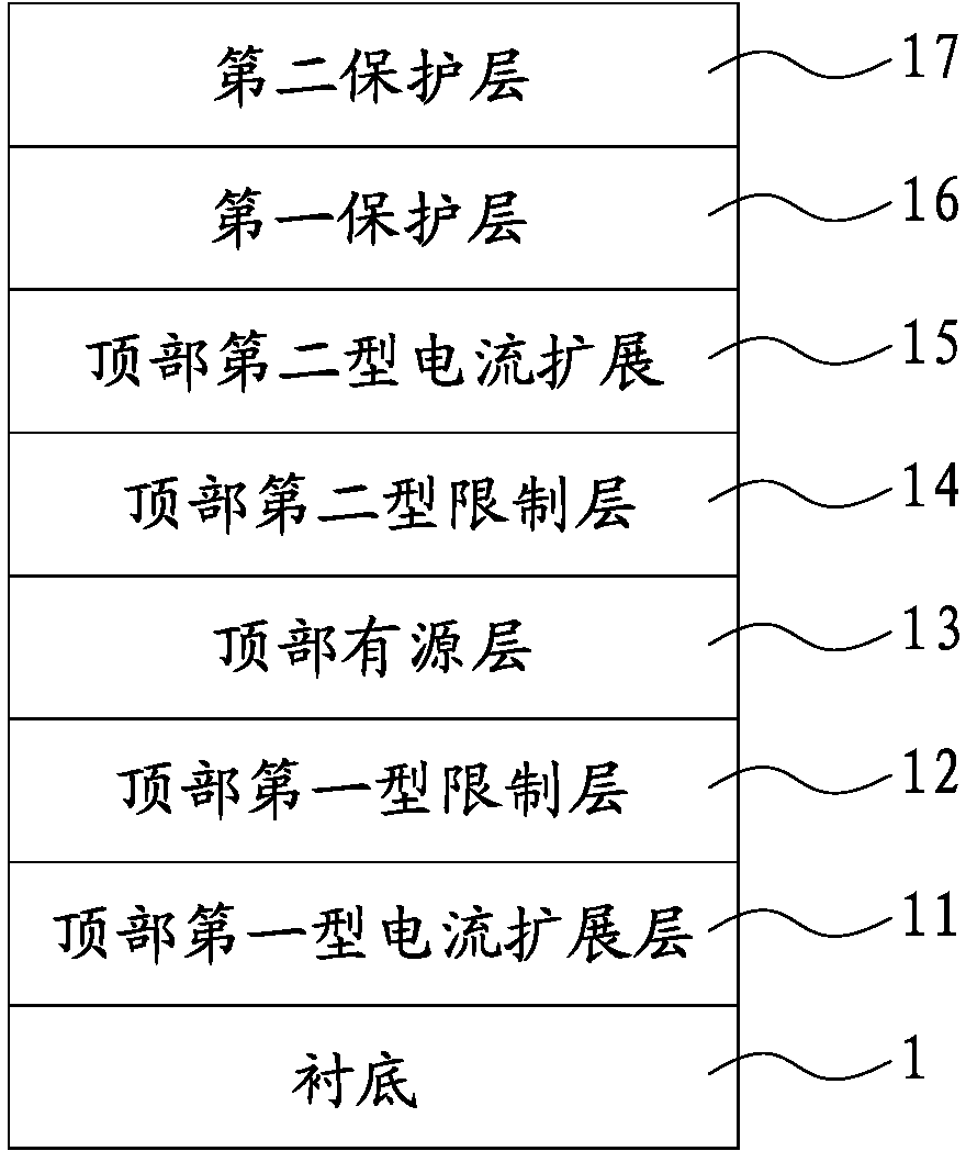
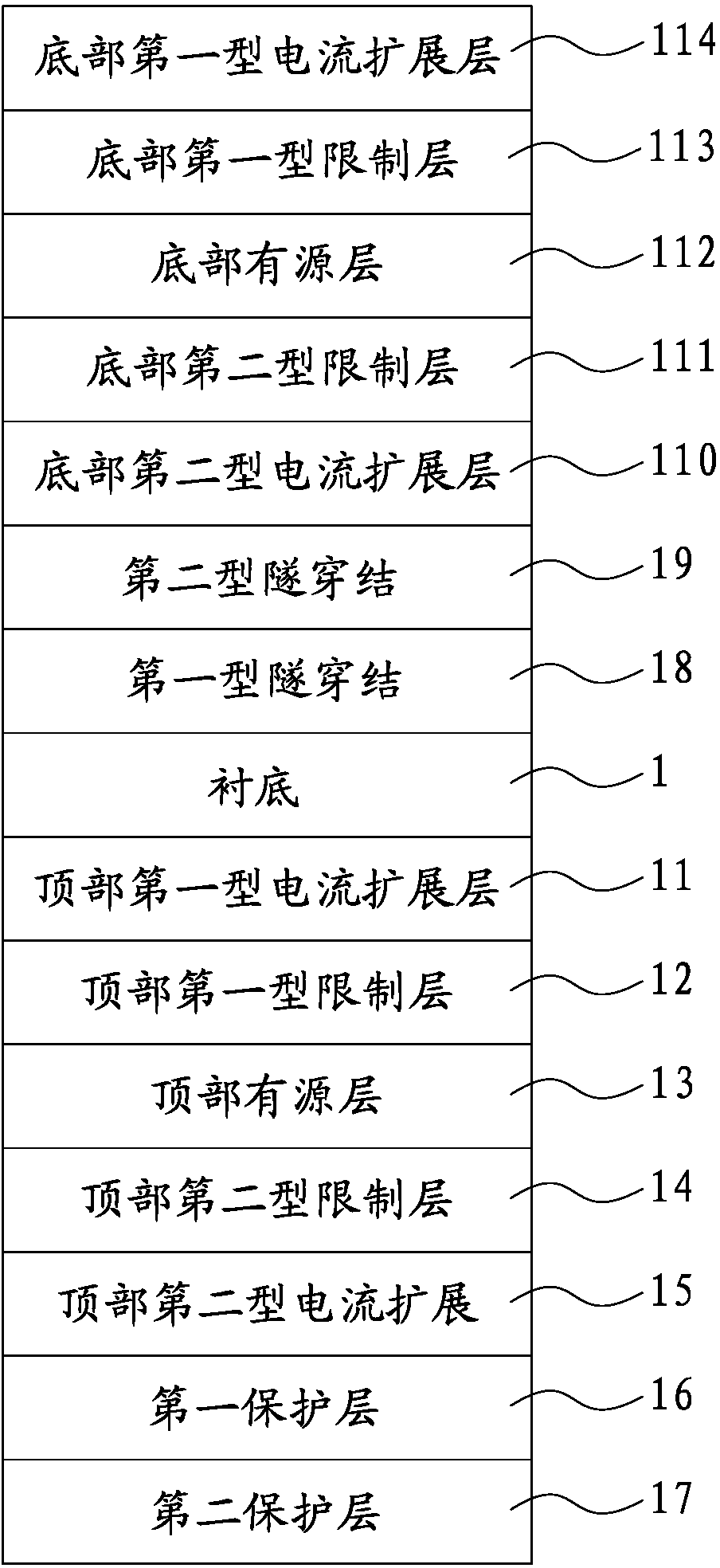
[0066] refer to Figure 1 to Figure 6 As shown, the first embodiment of the near-infrared light-emitting diode disclosed by the present invention, such as figure 1 The first epitaxial structure of the shown near-infrared light-emitting diode, the first epitaxial on the top of the AlGaAs substrate 1, from bottom to top, is the top first-type current spreading layer 11, the top first-type confinement layer 12, and the top has The source layer 13 , the top second-type confinement layer 14 , the top second-type current spreading layer 15 , the first protection layer 16 and the second protection layer 17 , the first protection layer 16 and the second protection layer 17 form a protection layer.
[0067] The substrate 1 is made of AlGaAs with 20% Al composition, the thickness is 300 μm, and it is doped with the first type, and the doping concentration is 1.0E+18. The quantum well of the top active layer 13 adopts the AlGaInAs / AlGaAs quantum well structure, the logarithm of the top ...
Embodiment 2
[0076] refer to Figure 7 to Figure 12 As shown, the second embodiment of the near-infrared light-emitting diode disclosed by the present invention, such as Figure 7 The first epitaxial structure of the shown near-infrared light-emitting diode, the first epitaxial on the top of the GaAs substrate 2, from bottom to top, is the top first-type current spreading layer 21, the top first-type confinement layer 22, and the top has The source layer 23 , the top second-type confinement layer 24 , the top second-type current spreading layer 25 , the first protection layer 26 and the second protection layer 27 , the first protection layer 26 and the second protection layer 27 form a protection layer.
[0077] Wherein, the substrate 2 has a thickness of 300 μm and is doped with the first type, and the doping concentration is 1.0E+18. The quantum well of the top active layer 24 adopts the quantum well structure of GaInAs / AlGaAs, the logarithm of the top quantum well is 3 pairs, and the l...
PUM
 Abstract
Description
Claims
Application Information


