Nano-column ultraviolet LED and preparation method and application thereof
A nano-column and ultraviolet technology, applied in nanotechnology, electrical components, circuits, etc., can solve the problems of low quantum efficiency and power of UV-LED, wide band gap of AlGaN material, and restrictions on the application of ultraviolet LED, so as to improve the light extraction efficiency , reduce light energy loss, and reduce the effect of quantum confinement Stark effect
- Summary
- Abstract
- Description
- Claims
- Application Information
AI Technical Summary
Problems solved by technology
Method used
Image
Examples
Embodiment 1
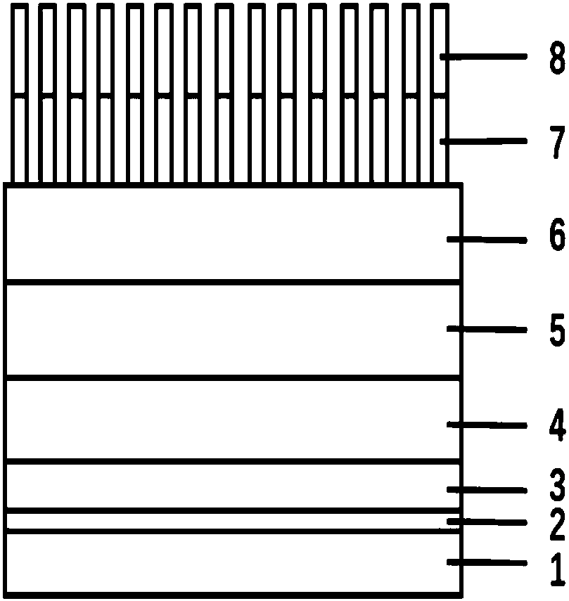
[0040] like figure 1 As shown, the nano-column ultraviolet LED of this embodiment includes a Si substrate 1, a pre-laid Al layer 2, an AlN layer 3, an AlGaN layer 4, a u-GaN layer 5, an n-GaN layer 6, and a quantum well from bottom to top. 7. p-GaN8.
[0041] The preparation method of described nanocolumn ultraviolet LED, comprises the following steps:
[0042] 1) Place the Si substrate in MOCVD, and epitaxially layer a pre-coated Al layer with a thickness of 3nm on the substrate: the substrate temperature is 900°C, the reaction chamber pressure is 50Torr, the rotation speed of the graphite disk is 1200r / min, and the TMAl The flow rate is 300sccm;
[0043] 2) A layer of AlN nucleation layer (AlN layer) with a thickness of 300nm is grown on the pre-coated Al layer obtained in step (1): the substrate temperature is 1200°C, the reaction chamber pressure is 60Torr, and the rotation speed of the graphite disk is 1200r / min , the flow rate of TMAl is 350sccm, NH 3 The flow rate i...
Embodiment 2
[0056] The nano-column ultraviolet LED of this embodiment includes a Si substrate, a pre-coated Al layer, an AlN layer, an AlGaN layer, a u-GaN layer, an n-GaN layer, a quantum well, and a p-GaN layer from bottom to top.
[0057] The preparation method of described nanocolumn ultraviolet LED, comprises the following steps:
[0058] 1) Place the Si substrate in MOCVD, and epitaxially layer a pre-coated Al layer with a thickness of 3nm on the substrate: the substrate temperature is 900°C, the reaction chamber pressure is 50Torr, the rotation speed of the graphite disk is 1200r / min, and the TMAl The flow rate is 300sccm;
[0059] 2) A layer of AlN nucleation layer (AlN layer) with a thickness of 300nm is grown on the pre-coated Al layer obtained in step (1): the substrate temperature is 1200°C, the reaction chamber pressure is 60Torr, and the rotation speed of the graphite disk is 1200r / min , the flow rate of TMAl is 350sccm, NH 3 The flow rate is 15slm;
[0060] 3) Grow a 600...
PUM
 Abstract
Description
Claims
Application Information


