PCB for LEDs, manufacturing method thereof, light emitting device and lamp

A photoresist, non-photosensitive technology, used in lighting devices, printed circuit manufacturing, lighting device parts and other directions, can solve the problems of difficult assembly of reflectors, unreliable structure, difficult processing, etc., and achieves easy automatic production and mass production. Simple and reliable production and assembly, the effect of reducing product cost

Inactive Publication Date: 2014-04-09
OSRAM GMBH
View PDF2 Cites 3 Cited by
  • Summary
  • Abstract
  • Description
  • Claims
  • Application Information

AI Technical Summary

Problems solved by technology

[0014] 1. The patterning of the reflective sheet needs to be formed by a punching machine, and different molds are required for different patterns, so the processing is difficult and the cost is high
[0015] 2. The assembly of the reflector is difficult and the reliability is low
The use of adhesives makes the structure unreliable, especially when working at high temperatures or after a long period of time
[0016] 3. Reflectors are usually cast and machined from expensive materials, making them expensive

Method used


Image

  • PCB for LEDs, manufacturing method thereof, light emitting device and lamp
  • PCB for LEDs, manufacturing method thereof, light emitting device and lamp
  • PCB for LEDs, manufacturing method thereof, light emitting device and lamp

Examples


Embodiment Construction

[0056] The present invention will be described more fully hereinafter with reference to the accompanying drawings that illustrate exemplary embodiments of the invention. This invention may, however, be embodied in many different forms and should not be construed as limited to the exemplary embodiments set forth herein. Rather, these exemplary embodiments are provided so that this disclosure will be thorough and complete, and will fully convey the scope of the invention to those skilled in the art.

[0057] Hereinafter, the present invention will be explained in detail with reference to the accompanying drawings.

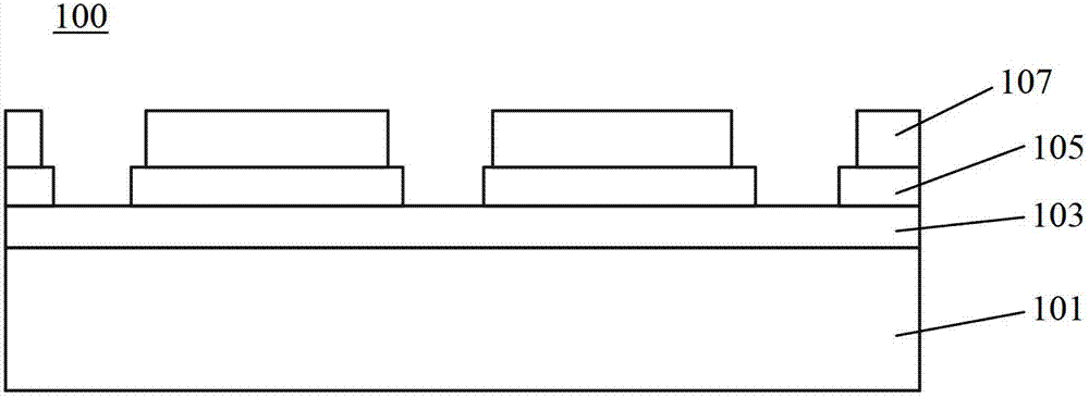
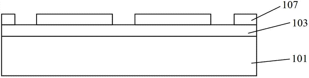
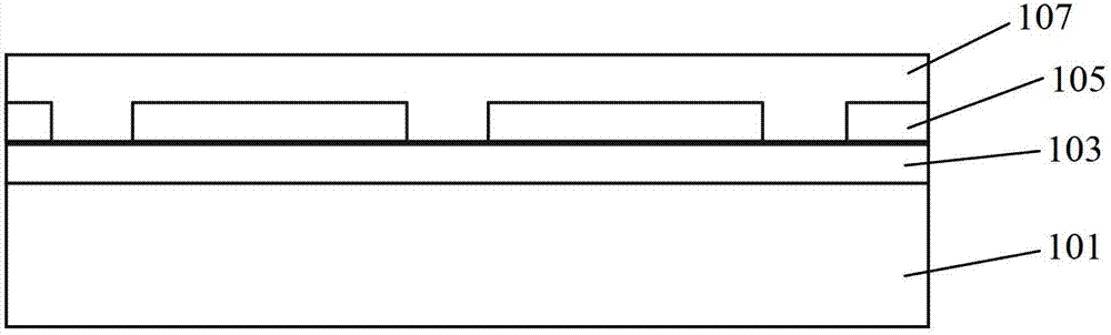
[0058] refer to Figure 4 , which shows a PCB 200 for LEDs according to an embodiment of the present invention. The PCB 200 includes an insulating base and a metal layer 205 . Generally, the insulating base may be composed of a substrate 201 and an insulating layer 203 above the substrate 201 . The metal layer 205 is preferably a copper layer, which is located ab...


PUM

PropertyMeasurementUnit
Thicknessaaaaaaaaaa

Abstract

The invention discloses a PCB for LEDs, a manufacturing method thereof, a light emitting device and a lamp. The PCB (200) for LEDs comprises insulating substrates (201, 203) and a metal layer (205) which is disposed above the insulating substrate (201) and provided with a pattern used for being electrically connected with an LED. The PCB (200) further comprises a reflective layer (207) made of non-photosensitive reflective material of which the reflectivity is greater than 80%, and the reflective layer is disposed on the metal layer so as to reflect light from the LED. According to the invention, absorption of light can be reduced, and the PCB is easy in automated production and mass production, simple in assembly and reliable.

Description

technical field [0001] The invention relates to a PCB used for LEDs and a manufacturing method thereof, a light emitting device, a light emitting device and a lamp. Background technique [0002] As a new light source, LED lamps have been widely used due to their advantages of high efficiency, pure light color, low energy consumption, long life, reliability and durability, no pollution, and flexible control. Currently, LED-based lamps have gradually replaced traditional light sources such as incandescent lamps, fluorescent lamps, HID lamps, and the like. [0003] For LED-based luminaires, one of the important components is the PCB (Printed Circuit Board). [0004] figure 1 A conventional PCB structure 100 is shown, which includes a substrate 101 and an insulating layer 103 , a copper layer 105 on the insulating layer 103 , and a solder mask 107 on the copper layer 105 . The LEDs will be electrically connected through a patterned copper layer 107 on the PCB for series / paral...

Claims


Application Information

Patent Timeline
IPC IPC(8): H05K1/18H05K3/30H01L33/62F21V23/00F21Y101/02
CPCH05K2201/2054H01L33/60H05K3/285H05K2201/10106
Inventor 郑盛梅张志超欧智君杨江辉
Owner OSRAM GMBH
Why Eureka
Try Eureka