Thin film transistor and manufacturing method thereof, array substrate and display device

A technology for thin film transistors and substrates, applied in transistors, semiconductor/solid-state device manufacturing, semiconductor devices, etc., can solve problems such as damage, deterioration of TFT performance, and complication of TFT manufacturing process.

Active Publication Date: 2014-04-16
BOE TECH GRP CO LTD
View PDF7 Cites 28 Cited by
  • Summary
  • Abstract
  • Description
  • Claims
  • Application Information

AI Technical Summary

Problems solved by technology

When the energy barrier at the interface is large and a Schottky contact is formed, it is easy to cause signal loss, thereby affecting the performance of the TFT
[0005] In addition, during the preparation process of the existing metal oxide TFT, when the source and drain metal layers above the metal oxide semiconductor active layer are etched in the subsequent process, the metal oxide semiconductor may be damaged. The active layer is damaged, which leads to the deterioration of TFT performance; therefore, an etching stopper layer is also provided above the metal oxide semiconductor active layer to prevent the subsequent preparation process from possibly affecting the metal oxide semiconductor. source damage
However, the increase of the etch barrier layer will complicate the TFT manufacturing process and increase the cost

Method used


Image

  • Thin film transistor and manufacturing method thereof, array substrate and display device
  • Thin film transistor and manufacturing method thereof, array substrate and display device
  • Thin film transistor and manufacturing method thereof, array substrate and display device

Examples


preparation example Construction

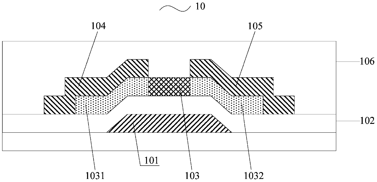
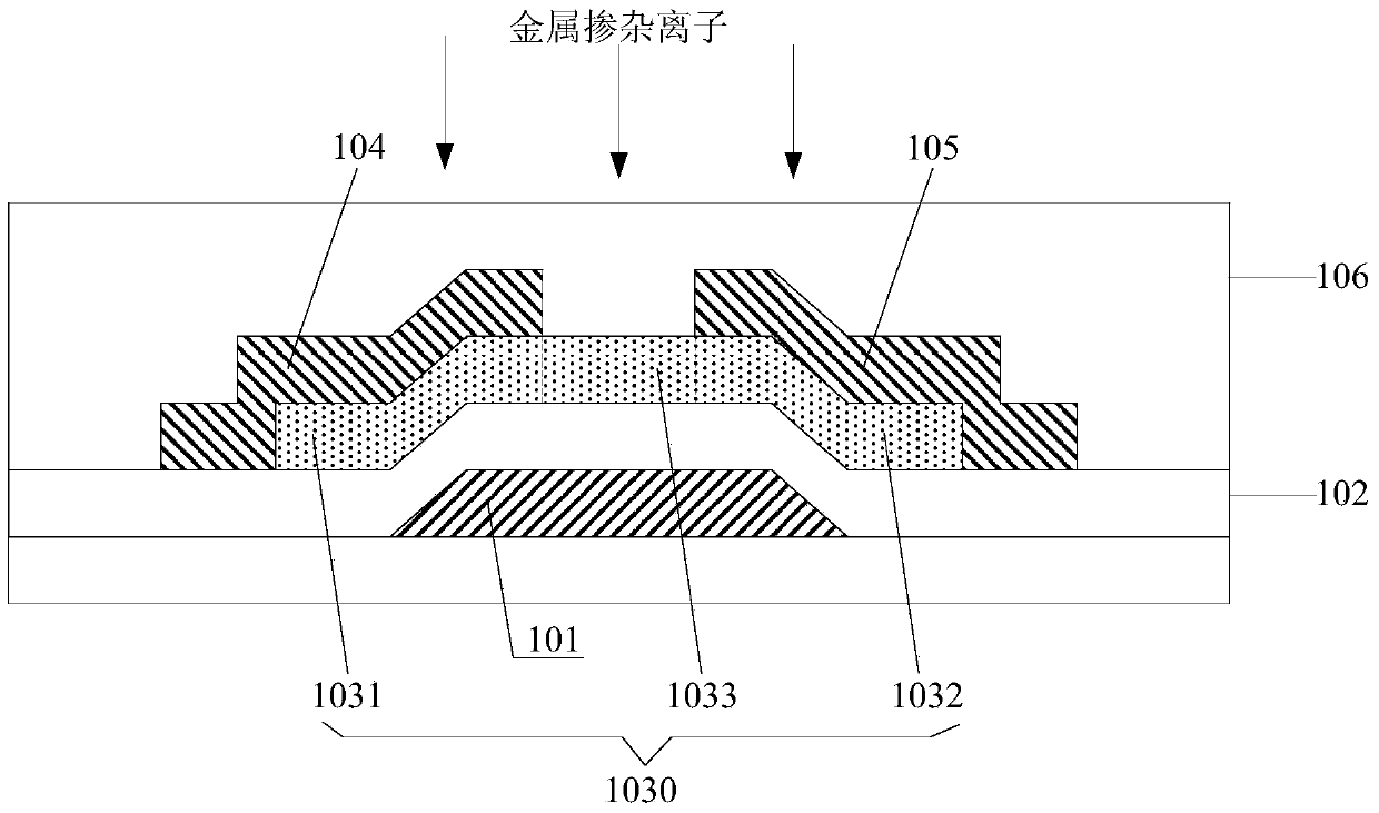
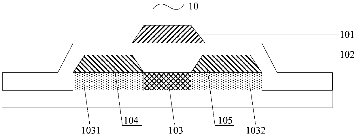
[0042] An embodiment of the present invention provides a method for manufacturing a thin film transistor 10 , which includes forming a gate 101 , a gate insulating layer 102 , a metal oxide semiconductor active layer 103 , a source 104 and a drain 105 on a substrate. The forming the metal oxide semiconductor active layer 103 on the substrate may include: forming an indium oxide-based binary metal oxide pattern layer 1030 on the substrate, the pattern layer including a first pattern 1031 corresponding to the source electrode 104 , the second pattern 1032 corresponding to the drain 105, and the third pattern 1033 corresponding to the gap between the source 104 and the drain 105, and the indium oxide-based binary metal oxide pattern Layer 1030 is in direct contact with the source electrode 104 and the drain electrode 105; the insulating layer formed above the source electrode 104 and the drain electrode 105 is used as a barrier layer, and the indium oxide based The elemental meta...


PUM


Abstract

The embodiment of the invention provides a thin film transistor and a manufacturing method of the thin film transistor, an array substrate and a display device, and relates to the technical field of display. The thin film transistor can solve the problem that the contact resistance exists between a source electrode and a semiconductor active layer and exists between a drain electrode and the semiconductor active layer, reduce the number of times of the picture composition technology and reduce the cost. The manufacturing method comprises the steps of forming a grid electrode, a grid insulating layer, the metal-oxide semiconductor active layer, the source electrode and the drain electrode on a substrate, wherein the formed metal-oxide semiconductor active layer comprises an indium-oxide series binary metal-oxide pattern layer making direct contact with the source electrode and the drain electrode, and a first pattern, a second pattern and a third pattern are included in the indium-oxide series binary metal-oxide pattern layer; using the insulating layer formed above the source electrode and the drain electrode as a barrier layer, adopting the ion implantation technology to implanting metal doping ions into the indium-oxide series binary metal-oxide pattern layer, conducting annealing treatment, converting the binary metal oxide of the third pattern into a polybasic metal-oxide semiconductor, and forming the metal-oxide semiconductor active layer. The thin film transistor is used for manufacturing the display device.

Description

technical field [0001] The invention relates to the field of display technology, in particular to a thin film transistor and a preparation method thereof, an array substrate, and a display device. Background technique [0002] With the continuous increase of the size of the display and the continuous increase of the frequency of the driving circuit, the mobility of the existing amorphous silicon thin film transistor has been difficult to meet the demand. [0003] High-mobility thin-film transistors (Thin Film Transistor, TFT) include polysilicon TFTs and metal oxide TFTs. However, the uniformity of polysilicon TFT is poor, the manufacturing process is complicated, and it is limited by equipment such as laser crystallization, which is not conducive to large-scale production; while the metal oxide TFT has high mobility, good uniformity, transparency, and simple manufacturing process, which can be better. It satisfies the needs of large-sized liquid crystal displays (Liquid Cr...

Claims


Application Information

Patent Timeline
Patent Type & Authority Applications(China)
IPC IPC(8): H01L21/28H01L29/786H01L21/336
CPCH01L21/426H01L29/66969H01L29/78693H01L29/78618H01L29/7869H01L21/02565H01L29/24H01L29/78606H01L27/1225
Inventor 赵策姜春生袁广才
Owner BOE TECH GRP CO LTD
Why Eureka
Try Eureka