A kind of semiconductor device structure and preparation method thereof

A device structure and semiconductor technology, applied in the direction of semiconductor devices, electrical solid devices, electrical components, etc., can solve the problem of high contact resistance and achieve the effect of low contact resistance

Inactive Publication Date: 2018-07-20
CHANGXIN MEMORY TECH INC
View PDF5 Cites 0 Cited by
  • Summary
  • Abstract
  • Description
  • Claims
  • Application Information

AI Technical Summary

Problems solved by technology

[0007] In view of the above-mentioned shortcomings of the prior art, the object of the present invention is to provide a semiconductor device structure and its preparation method, which is used to solve the problem of high contact resistance formed between the device structure and the silicon material in the prior art, etc.

Method used


Image

  • A kind of semiconductor device structure and preparation method thereof
  • A kind of semiconductor device structure and preparation method thereof
  • A kind of semiconductor device structure and preparation method thereof

Examples


Embodiment 1

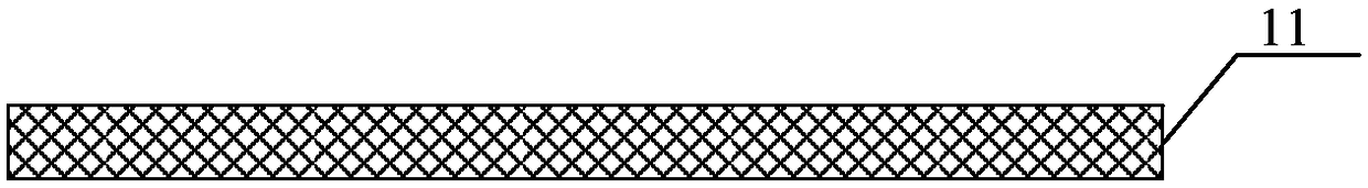
[0065] see Figure 1 ~ Figure 4 , the present embodiment provides a method for preparing a semiconductor device structure, the preparation method comprising the following steps:

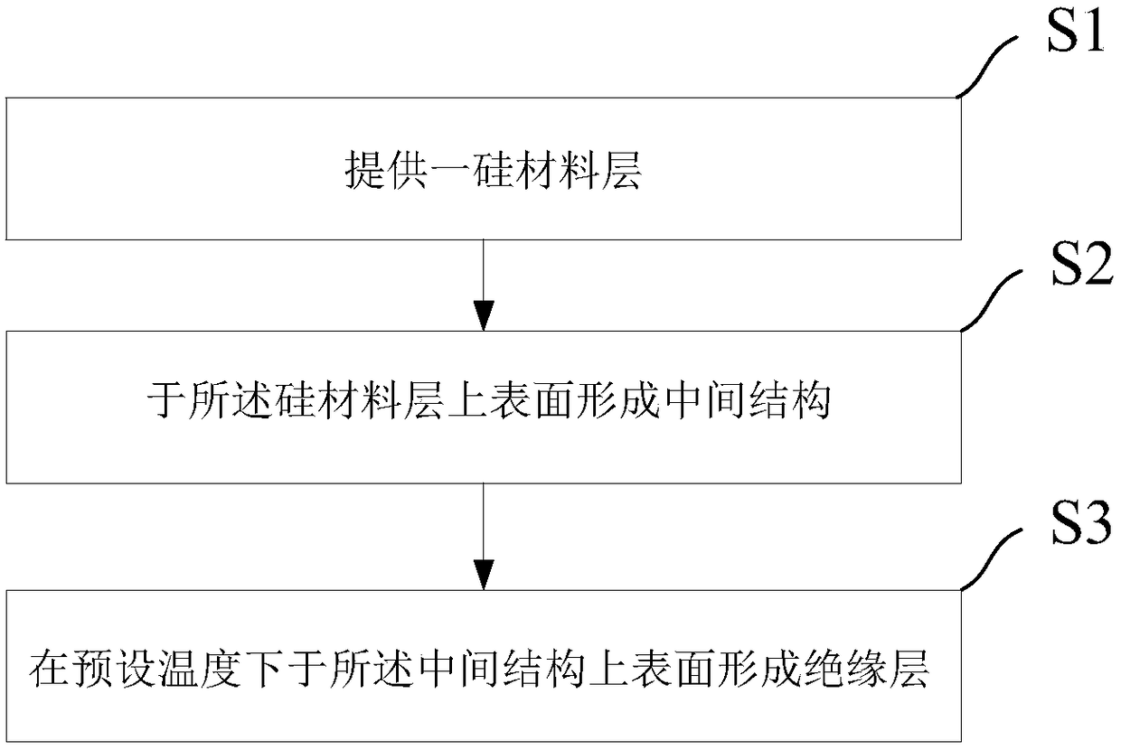
[0066] Such as figure 1 S1 and figure 2 Shown, carry out step 1), provide a silicon material layer 11;

[0067] Specifically, the silicon material layer 11 can be any silicon-containing material, including single crystal silicon, polycrystalline silicon, amorphous silicon, or silicon germanium material, such as the silicon material layer 11 is a polycrystalline silicon germanium layer, the silicon The material of the material layer 11 may also be a doped material of any of the above materials, such as intrinsic silicon, P-type silicon, N-type silicon, etc., which are not specifically limited here. Of course, the silicon material layer 11 can also be a laminated structure of at least two layers of materials, such as a laminated structure composed of a polysilicon layer doped with N-type impurities...

Embodiment 2

[0085] see Figure 5 , this embodiment provides a method for fabricating a semiconductor device structure. The difference between the second embodiment and the first embodiment is that in step 2), the intermediate structure 12 further includes a first metal nitride layer 122, and the A first metal nitride layer 122 is formed between the first metal layer 121 and the second metal layer 124 .

[0086] Specifically, the material of the first metal nitride layer 122 includes but not limited to tantalum nitride, palladium nitride, platinum nitride, cobalt nitride, zirconium nitride, nickel nitride, titanium nitride, molybdenum nitride, And the first metal nitride layer 122 is formed by physical vapor deposition (PVD) method (such as evaporation, electroplating or sputtering, etc.), chemical vapor deposition (CVD) method or atomic layer deposition (ALD) method. In addition, the thickness of the first metal nitride layer 122 is 3-50 nm, preferably 5-30 nm or 10-20 nm. In this embodi...

Embodiment 3

[0100] see Figure 6 , this embodiment provides a method for fabricating a semiconductor device structure. The difference between the third embodiment and the second embodiment is that in step 2), the intermediate structure 12 further includes a second metal nitride layer 125, and the The second metal nitride layer 125 is formed between the first metal nitride layer 122 and the second metal layer 124 .

[0101] Specifically, the material of the second metal nitride layer 125 may be tungsten nitride, or W / Si / N-based materials, etc., and the second metal nitride layer 125 is formed by physical vapor deposition (PVD) (such as evaporation, electroplating or sputtering, etc.), chemical vapor deposition (CVD) or atomic layer deposition (ALD) methods. In addition, the thickness of the second metal nitride layer 125 is 1-6 nm, preferably 2-4 nm. In this embodiment, the thickness of the second metal nitride layer 125 is 3 nm.

[0102] It should be noted that, in this embodiment, poly...


PUM

PropertyMeasurementUnit
thicknessaaaaaaaaaa
thicknessaaaaaaaaaa
thicknessaaaaaaaaaa

Abstract

The present invention provides a semiconductor device structure and preparation method. The preparation method includes steps: providing a silicon material layer; forming an intermediate structure on the silicon material layer, at least the first metal layer, and the first metal layer is formed in the silicon materialOn the surface of the layer, the intermediate structure also includes the second metal layer, the second metal layer is formed on the first metal layer, and the material of the second metal layer is different from the material of the first metal layer;The insulation layer is formed on the upper surface, and during the formation of the insulation layer, the silicon element of the first metal layer and the silicon material layer reacts at the preset temperature to generate the first siliconized metal layer.Through the above technical solutions, the semiconductor device structure of the present invention can form a lower contact resistance with silicon materials; the semiconductor device structure of the present invention can directly be the most high -temperature -resistant wire; the semiconductor structure of the present invention can solve the stack grille structureThe problem of contact resistance and ensure the efficiency of the stack grille structure.

Description

technical field [0001] The invention belongs to the technical field of integrated circuit manufacturing, and in particular relates to a semiconductor device structure with a wire having a multilayer film structure and a preparation method thereof. Background technique [0002] In today's semiconductor industry, silicon material is the main semiconductor substrate used to manufacture electronic components such as transistors and secondary bodies. Its advantages are: 1) low cost; 2) silicon dioxide can be generated during thermal oxidation , wherein silicon dioxide is a strong and stable dielectric film; 3) silicon materials can withstand higher operating temperatures and larger doping ranges. [0003] Due to the wide application of silicon materials, it is necessary to find a material that can form a low-resistance contact layer with silicon materials. If the contact layer can also be directly used as a wire, the complexity of the manufacturing process can be saved. In the p...

Claims


Application Information

Patent Timeline
Patent Type & Authority Patents(China)
IPC IPC(8): H01L21/28H01L29/423H01L29/45
CPCH01L29/401H01L29/42324H01L29/456H01L29/40114H10B41/30H01L29/4975
Inventor 不公告发明人
Owner CHANGXIN MEMORY TECH INC
Why Eureka
Try Eureka