Optical waveguide parameter test fixture

A parametric testing and optical waveguide technology, applied in the field of optical waveguides, can solve the problems of increasing test difficulty and detector requirements, inability to adjust the gap between the bottom surfaces of prisms, low coupling efficiency of optical waveguides, etc., to achieve reliable transmission loss, simple structure, test high precision effect

Inactive Publication Date: 2015-09-09
SHENZHEN GRADUATE SCHOOL TSINGHUA UNIV
View PDF6 Cites 0 Cited by
  • Summary
  • Abstract
  • Description
  • Claims
  • Application Information

AI Technical Summary

Problems solved by technology

Therefore, the research and development of the optical waveguide parameter test fixture is known to be concerned by relevant researchers. For example, the patent document CN 101839799A discloses an optical waveguide test device, which is mainly used for clamping the optical waveguide to be tested and the prism coupler, but the device directly Pressing the prism on the surface of the optical waveguide cannot adjust the gap between the bottom surface of the prism and the surface of the optical waveguide to be tested. The coupling efficiency of the optical waveguide is very low, which increases the difficulty of testing and the requirements of the detector, and the test accuracy will also be affected.
Moreover, the output coupling prism of this device cannot be moved, and the optical waveguide fixture can only hold a fixed-sized optical waveguide to be tested and there is no light-through space reserved on the bottom surface, so the applicable test methods of this device are limited.

Method used


Image

  • Optical waveguide parameter test fixture
  • Optical waveguide parameter test fixture
  • Optical waveguide parameter test fixture

Examples


example 1

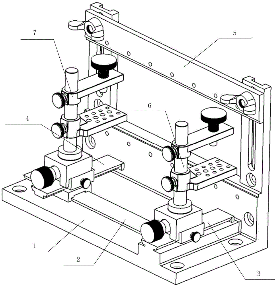
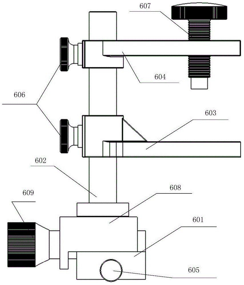
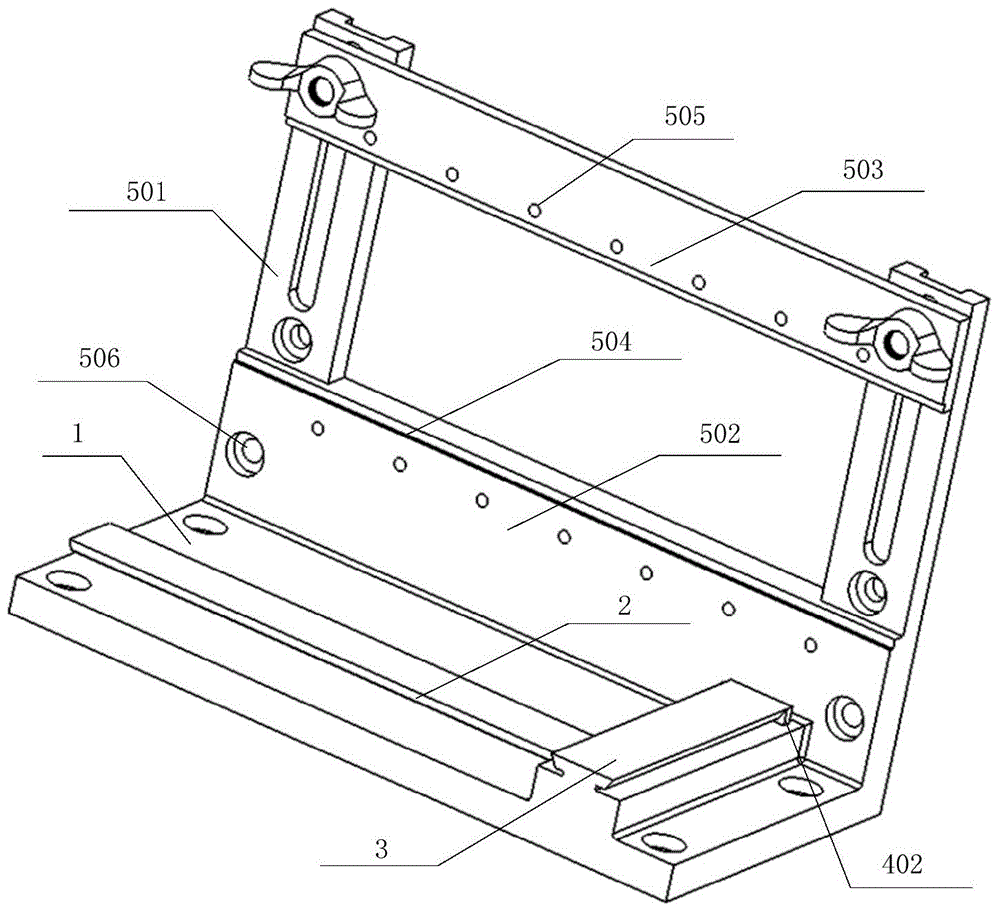
[0059] Stainless steel or aluminum alloy is used as the manufacturing material, and standard parts such as set screws, lag screws and wing nuts are selected. The base is L-shaped, 120mm long, 60mm wide, 8mm thick, and 24mm high. The length of the longitudinal rail 2 is 90mm, the length of the fixed horizontal rail 3 and the sliding horizontal rail 4 are both 48 mm. The plane of the sliding horizontal rail 4 and the longitudinal rail 2 on the longitudinal rail 2 coincide with the plane of the fixed horizontal rail 3. The vertical sliding guide 501 of the optical waveguide clamp 5 has a length of 54 mm, a width of 15 mm, and a thickness of 5 mm. The sliding support plate 503 is 120mm long, 15mm wide, and 3mm thick. The threaded holes on the fixed support plate 502 and the sliding support plate 503 are M5, and the limit step is 2mm×0.5mm. The size of the prism is 20mm×20mm×20mm, and the optical waveguide to be tested is 50mm×30mm×0.5mm. The incident light is 1550nm wavelength i...

example 2

[0062] CCD digital camera method is used to measure the loss of optical waveguide. Remove the output prism fixture 7 and excite the optical waveguide light by retaining the prism coupler held by the input prism fixture 6. The schematic diagram of the test principle is as follows Image 6 Shown. After collecting the light intensity data reflected in the photos taken by the CCD camera 8 with the image acquisition card, digital image processing technology is used to filter and reduce noise, and the transmission light intensity change graph of the optical waveguide light in the optical waveguide layer can also be drawn, so as to obtain Obtain the transmission loss of the optical waveguide to be measured.


PUM


Abstract

The invention relates to an optical waveguide parameter testing clamp which comprises a base, an optical waveguide clamp, a longitudinal guiderail, a set of fixed transverse guiderails, an input prism clamp, a set or multiple sets of slide transverse guiderails and an output prism clamp. The fixed transverse guiderails, the longitudinal guiderails and the optical waveguide clamp are mounted on the base. The slide transverse guiderails are mounted on the longitudinal guiderail. The input prism clamp is mounted on the fixed transverse guiderails. The output prism clamp is mounted on the slide transverse guiderails. The optical waveguide clamp is located at the position close to the tail ends of the fixed transverse guiderails and the slide transverses guiderails. The output prism clamp can be replaced by a CCD camera. The optical waveguide parameter testing clamp can be used for clamping prism couplers, to-be-tested waveguides, detectors and the like. In addition, the optical waveguide parameter testing clamp is applicable to various waveguide parameter measuring methods, novel and simple in structure, high in testing precision, good in repeatability, convenient to operate, wide in application range, and the like.

Description

Technical field [0001] The invention relates to the technical field of optical waveguides, in particular to an optical waveguide parameter test fixture, which is used for the measurement of optical waveguide parameters such as the transmission loss, refractive index and distribution of the optical waveguide and its devices, and the thickness of the waveguide layer. Background technique [0002] The optical waveguide is the most basic unit of the integrated optical circuit and its components. It is the most potential basic structure for the realization of optoelectronic integration and photonic devices. Its function is similar to the wire in the circuit, which is used to realize the optical path connection between different devices. Light waves mainly play the role of restriction, transmission, and coupling. Due to the small propagation loss, the production cost is low, and it is easy to integrate with other optoelectronic components. In order to improve the performance of variou...

Claims


Application Information

Patent Timeline
Patent Type & Authority Patents(China)
IPC IPC(8): B25B11/00
CPCB25B11/00
Inventor 董瑛袁登鹏
Owner SHENZHEN GRADUATE SCHOOL TSINGHUA UNIV
Why Eureka
Try Eureka