Method for designing mapping scheme and topological structure between task and node in on-chip network

A mapping scheme and network-on-chip technology, applied to general-purpose stored program computers, etc., can solve problems such as not being able to better reflect the actual situation

Inactive Publication Date: 2014-04-30
UNIV OF ELECTRONICS SCI & TECH OF CHINA
View PDF2 Cites 8 Cited by
  • Summary
  • Abstract
  • Description
  • Claims
  • Application Information

AI Technical Summary

Problems solved by technology

This method can only be randomly arranged when dealing with the schemes with the same aggregation distance, which cannot reflect the actual situation well.

Method used


Image

  • Method for designing mapping scheme and topological structure between task and node in on-chip network
  • Method for designing mapping scheme and topological structure between task and node in on-chip network
  • Method for designing mapping scheme and topological structure between task and node in on-chip network

Examples


Embodiment Construction

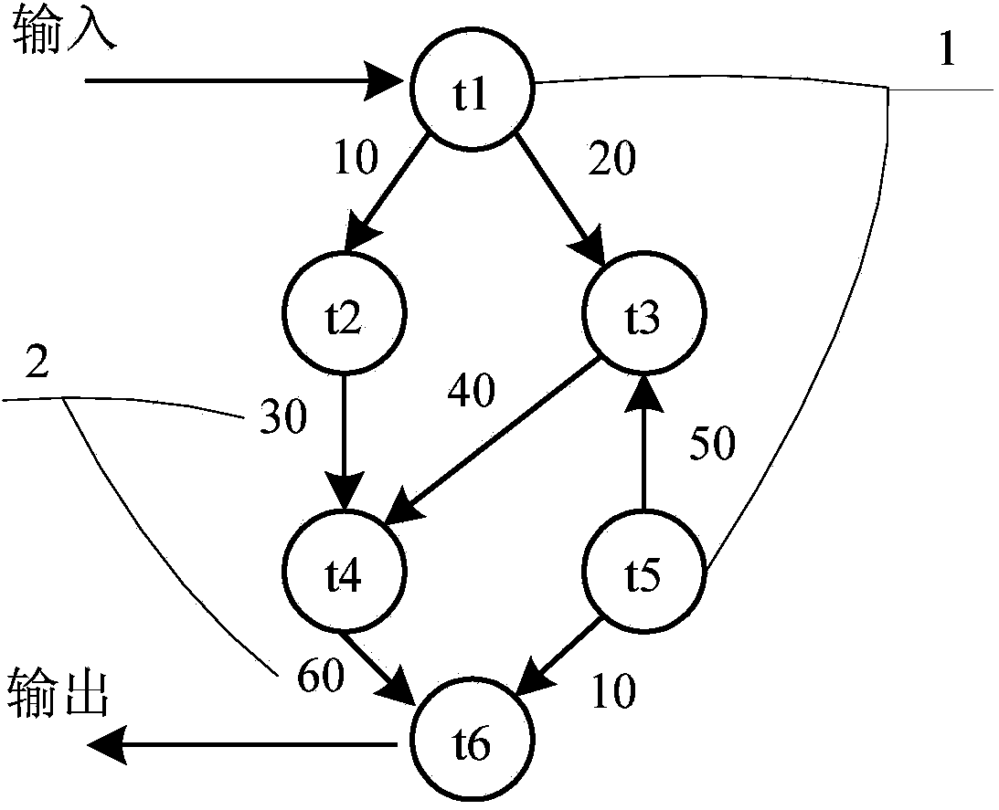
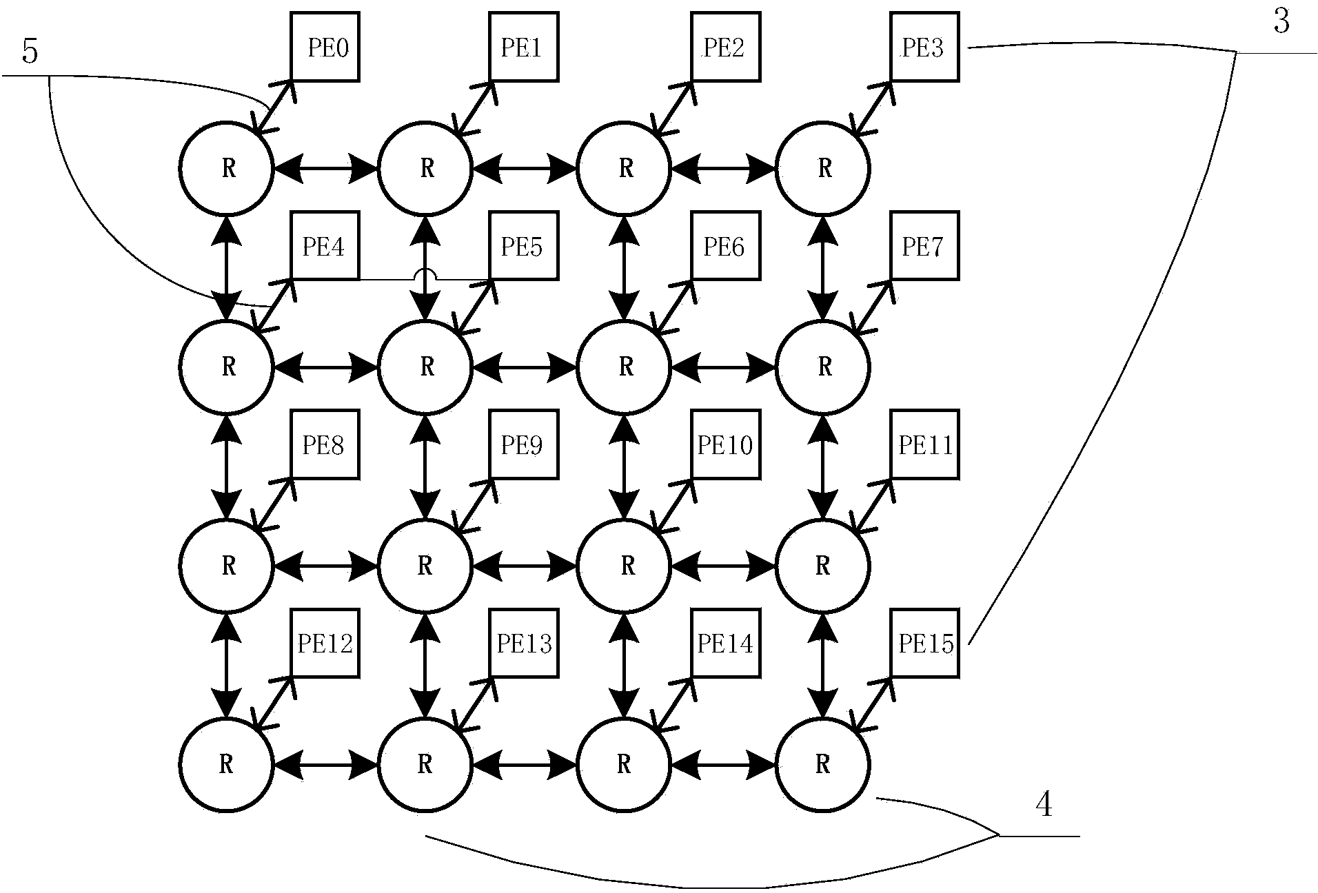
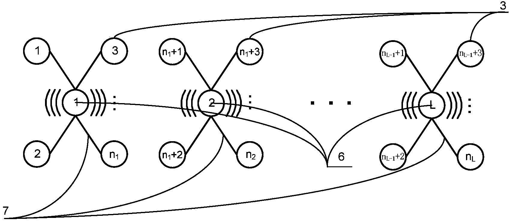
[0072] The present invention will be further described in detail below in combination with specific embodiments. However, it should not be understood that the scope of the above subject matter of the present invention is limited to the following embodiments, and all technologies realized based on the content of the present invention belong to the scope of the present invention.

[0073] The present invention separates power consumption and response time as the priority index of the assessment scheme, but considers power consumption and response time at the same time in the process of finding the optimal scheme, so that the found scheme minimizes power consumption and system delay at the same time, Therefore, the performance of the network designed by using this optimized scheme is the best, and compared with other methods for finding the priority scheme of mapping between tasks and nodes under multiple objective functions, it has the characteristics of complexity and simple imp...


PUM


Abstract

The invention discloses a method for designing a mapping scheme and a topological structure between a task and a node in an on-chip network. The method is characterized by comprising the steps that power consumption and response time are separated and used as preferential indexes for an appraisal program, the power consumption and the response time are simultaneously considered in the process of finding the optimal scheme, the aim of enabling the power consumption and the response time to be simultaneously minimum through the found scheme is achieved, and in addition, the topological structure enabling the power consumption and the response time to be minimum is selected.

Description

technical field [0001] The invention relates to the field of integrated circuit design, in particular to a design method for mapping schemes and topological structures between tasks and nodes in a wireless on-chip network for multi-tasks and multi-nodes in an on-chip network. Background technique [0002] With the increasing computational complexity of communication terminals and equipment in the future, the demand for integration scale of real-time complex system chips will increase rapidly. Dozens or hundreds of processing units may be integrated on one chip, and signal processing based on multi-core Platform becomes the development trend of software defined radio. In such an integrated system, designing a reliable, high-speed, low-power-consumption high-performance on-chip communication system has become a challenge and an opportunity for the development of a System on Chip (SoC). The bus communication structure of the traditional multi-core SoC cannot meet the data exch...

Claims


Application Information

Patent Timeline
Patent Type & Authority Applications(China)
IPC IPC(8): G06F15/76
Inventor 陈亦欧胡剑浩凌翔
Owner UNIV OF ELECTRONICS SCI & TECH OF CHINA
Why Eureka
Try Eureka