Manufacturing method of X-ray flat panel detector

A technology of flat panel detection and manufacturing method, which is applied to radiation control devices and other directions, can solve the problems of breakdown of amorphous silicon thin film transistors, large charge changes, and lower production yields of X-ray flat panel detection devices, so as to improve production yields. Effect

Active Publication Date: 2014-05-07
SHANGHAI TIANMA MICRO ELECTRONICS CO LTD
View PDF3 Cites 13 Cited by
  • Summary
  • Abstract
  • Description
  • Claims
  • Application Information

AI Technical Summary

Problems solved by technology

Since the drain electrode 150b is electrically connected to the data line 120, the generated charge can be released through the data line 120; while the bottom electrode 160 (source electrode 150a) is relatively isolated, and the amount of charge change is very large, Therefore, the bottom electrode 160 (source electrode 150a) can only discharge charges through the formation of a tip discharge at the edge of the active layer 140 and the gate 130, which

Method used


Image

  • Manufacturing method of X-ray flat panel detector
  • Manufacturing method of X-ray flat panel detector
  • Manufacturing method of X-ray flat panel detector

Examples


Embodiment 1

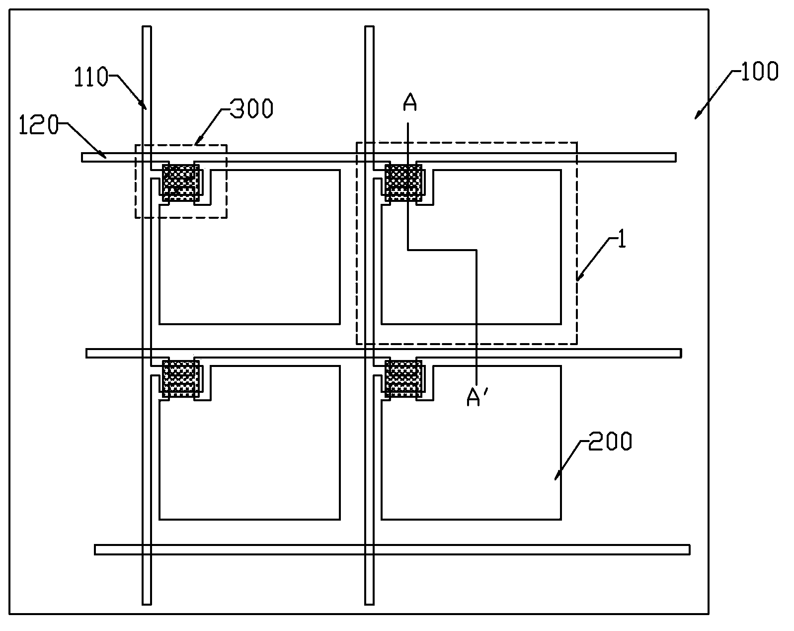
[0081] First, if Figure 4 As shown, a substrate 100 is provided, and the substrate 100 is a glass substrate 100. The material of the substrate 100 of the present invention is not limited to glass, but can also be high temperature resistant organic matter, metal, quartz or diamond, or other materials that can withstand the TFT process To implement temperature, the surface of the panel is flat. The first conductive layer is sputtered on the substrate 100, and then a photoresist is coated on the first conductive layer, and the photoresist is exposed using a mask plate with a specific pattern, and the patterned the first conductive layer; then wet etching the first conductive layer to form the gate 130 and the scanning lines; finally, stripping the photoresist and cleaning it. Wherein, the first conductive layer may be made of metal materials such as aluminum, neodymium, molybdenum, chromium and alloys thereof.

[0082] Next, if Figure 5 As shown, the gate insulating layer 13...

Embodiment 2

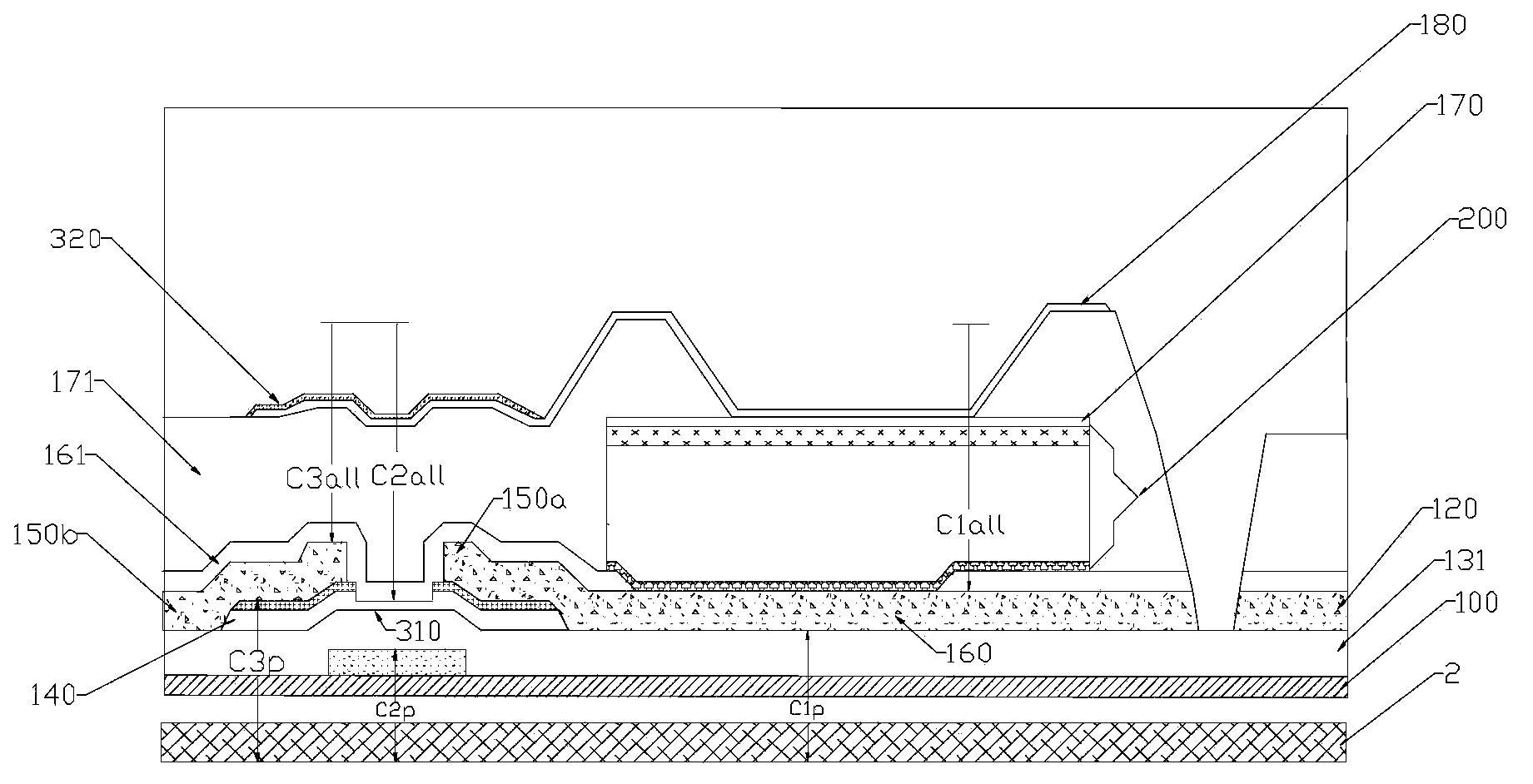
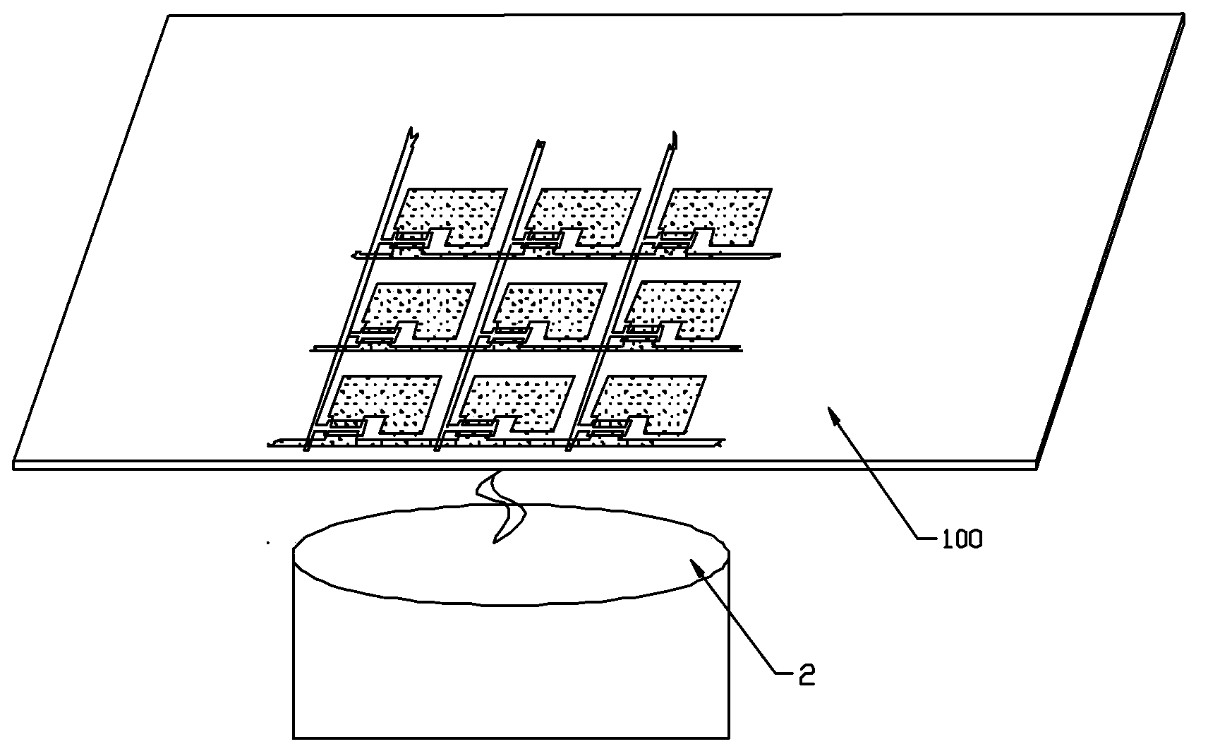
[0094] Compared with Embodiment 1, in this embodiment, the bottom electrode 160 (source electrode 150 a ) of the photoelectric conversion element 200 is electrically connected to the scanning line through the connection part 190 as a whole. At the moment when the support pillar 2 contacts or separates from the bottom surface of the substrate 100 , a large amount of electrostatic charge generated by the bottom electrode 160 (source electrode 150 a ) is discharged through the scanning line. The manufacturing steps before the deposition of the gate insulating layer 131 and after the formation of the first passivation layer 161 are the same or similar to those of the first embodiment, and will not be repeated here. The differences of this embodiment will be described in detail below with reference to the drawings.

[0095] After forming the silicon islands of the active layer 140, as Figure 14 As shown, the gate insulating layer is patterned, and a part of the scan line 110 is ex...


PUM


Abstract

The invention discloses a manufacturing method of an X-ray flat panel detector. The method comprises the following steps: providing a substrate; forming a thin film transistor, a bottom electrode and a conductive element on the substrate, wherein the bottom electrode and the conductive element are electrically connected as a whole through a connecting part; forming a photoelectric conversion element and a top electrode on the bottom electrode; and forming a shading layer above a channel of the thin film transistor and etching the connecting part to disconnect the bottom electrode and the conductive element. According to the method, the bottom electrode (the source) and the conductive element are electrically connected as a whole through the connecting part, and when manufacture of the thin film transistor is completed, static electricity produced by the bottom electrode (the source) is released through the conductive element at the moment when a supporting column contacts or is separated from the bottom surface of the substrate in the subsequent manufacturing process so as to avoid electrostatic breakdown of the thin film transistor.

Description

technical field [0001] The invention relates to the technical field of digital imaging, in particular to a manufacturing method of an X-ray flat panel detection device. Background technique [0002] X-ray Flat Panel Detector (X-ray Flat Panel Detector) has the advantages of clear and delicate images, high resolution, wide gray scale, large amount of information, and large dynamic range, and is widely used in medical, industrial and other fields. The X-ray flat-panel detection device is mainly composed of a scintillator or phosphor layer, an amorphous silicon layer (a-Si) with a photodiode function, and a thin film transistor (Thin film transistor, TFT) array. The principle is that after the scintillator or phosphor layer is exposed to X-rays, the X-ray photons are converted into visible light, and then the amorphous silicon layer with a photodiode function is converted into an image electrical signal, and finally a digital image is obtained. [0003] Such as figure 1 As sh...

Claims


Application Information

Patent Timeline
IPC IPC(8): H01L27/146
Inventor 肖文文朱虹凌严祁刚
Owner SHANGHAI TIANMA MICRO ELECTRONICS CO LTD
Why Eureka
Try Eureka