Semiconductor device with super junction structure

A semiconductor and device technology, applied in the field of semiconductor devices with super junction structure, can solve problems affecting production yield, process complexity, increased cost, etc., to improve withstand voltage capability and work stability, improve device reliability, The effect of increasing the lateral pressure resistance

Inactive Publication Date: 2014-05-07
XIAN SEMIPOWER ELECTRONICS TECH
View PDF6 Cites 11 Cited by
  • Summary
  • Abstract
  • Description
  • Claims
  • Application Information

AI Technical Summary

Problems solved by technology

In the related prior art, some designers propose to change the width ratio of the P / N region in the terminal withstand voltage region, and some designers propose to use low-concentration doping in the terminal withstand voltage region, but these methods will bring process The complexity on the surface increases the cost and even affects the production yield

Method used


Image

  • Semiconductor device with super junction structure
  • Semiconductor device with super junction structure
  • Semiconductor device with super junction structure

Examples


Embodiment Construction

[0023] The present invention will be further described in detail below in conjunction with specific embodiments, which are explanations of the present invention rather than limitations.

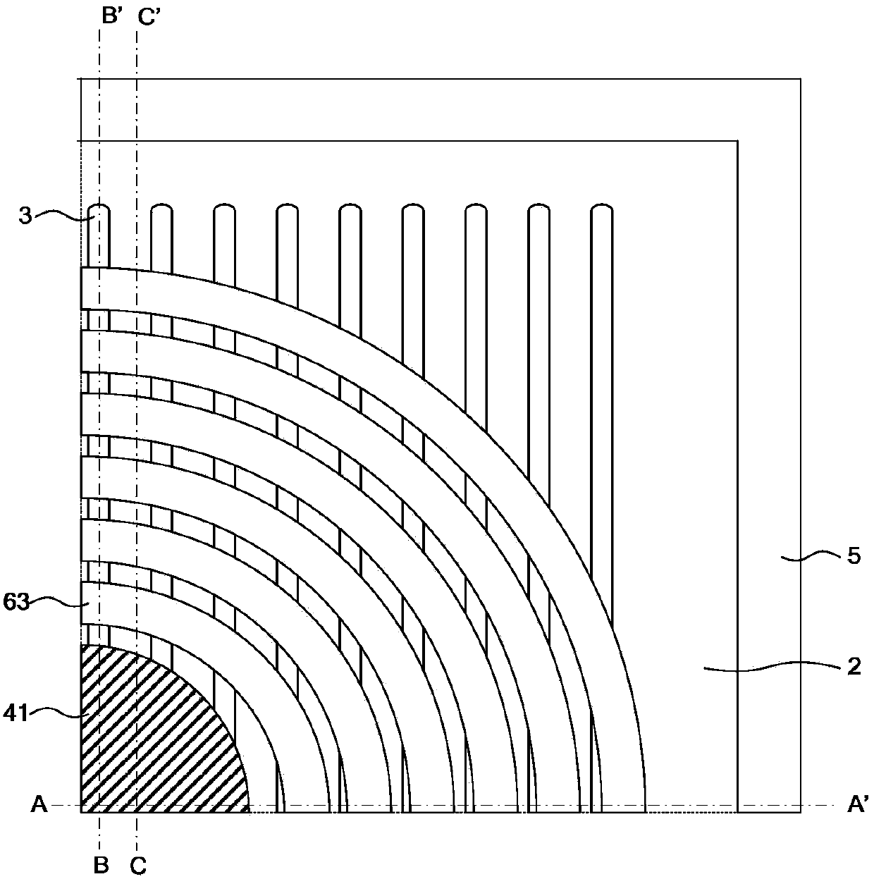
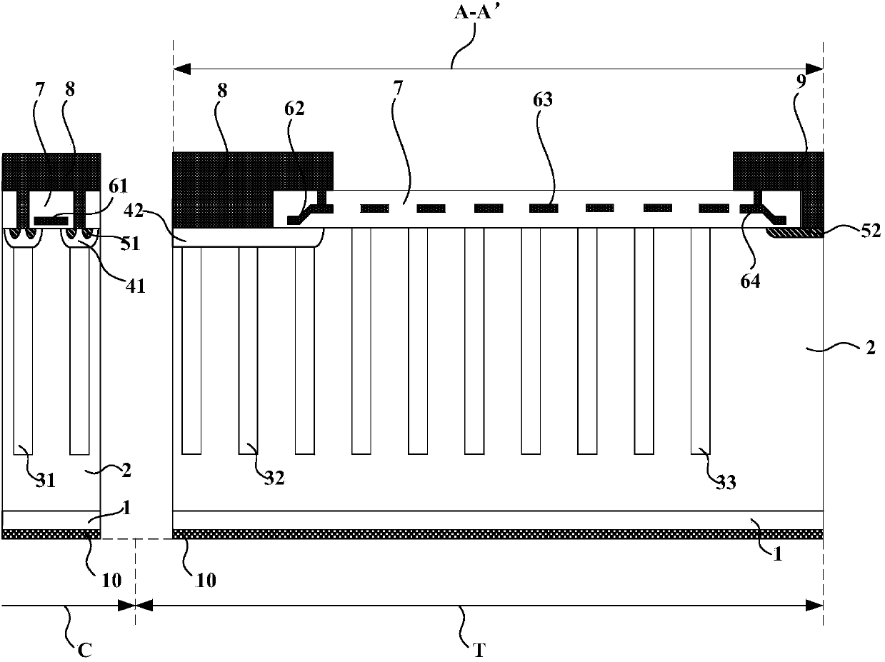
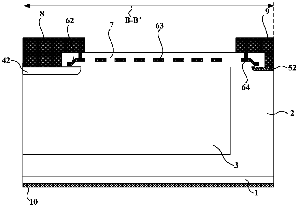
[0024] The present invention is a semiconductor device with a super junction structure, such as figure 2 As shown, it includes an N-type doped semiconductor substrate 1 and an N-type doped epitaxial layer 2 arranged in sequence from bottom to top; the N-type doped epitaxial layer 2 is internally provided with a P-type filled well region 3, and the P-type filled well Region 3 includes a first P-type filled well region 31, a second P-type filled well region 32, and a third P-type filled well region 33 arranged from the inside to the outside with the same structure; the upper side of the first P-type filled well region 31 is set There is a first P-type doped region 41, an N-type doped region 51 is arranged in the first P-type doped region 41, and a second P-type doped region 42 is arranged on t...


PUM


Abstract

The invention provides a semiconductor device with a super junction structure. The semiconductor device comprises an N-type doped semiconductor substrate and an N-type doped epitaxial layer, wherein the N-type doped semiconductor substrate and the N-type doped epitaxial layer are sequentially arranged from bottom to top, and a first P-type filling well region, a second P-type filling well region and a third P-type filling well region are arranged inside the N-type doped epitaxial layer. A first P-type doping region is arranged on the upper side of the first P-type filling well region and provided with an N-type doping region, and a second P-type doping region is arranged on the upper side of the second P-type filling well region. A terminal pressure-withstanding structure T is arranged on the periphery of a primitive cell source electrode region C, wherein the terminal pressure-withstanding structure T comprises the second P-type filling well region, the second P-type doping region, the third P-type filling well region and the corresponding part of the N-type doped epitaxial layer, and the primitive cell source electrode region C comprises the first P-type filling well region, the first P-type doping region, the N-type doping region and the corresponding part of the N-type doped epitaxial layer. The parts, corresponding to polycrystalline silicon arranged in a part of dielectric layer above a gate oxide layer, of the terminal pressure-withstanding structure T and the primitive cell source electrode region C form a gate electrode structure and a polycrystalline silicon field plate structure respectively.

Description

technical field [0001] The invention belongs to the technical field of semiconductor power devices, and relates to a high-voltage power device, in particular to a semiconductor device with a super junction structure. Background technique [0002] Traditional vertical high-voltage power devices use a low-doped epitaxial drift layer as a voltage support layer, and its on-resistance is mainly the resistance of the drift layer. The withstand voltage capability of the drift layer is determined by its thickness and doping concentration. Therefore, in order to increase the breakdown voltage, it is necessary to increase the thickness of the drift layer and reduce its doping concentration at the same time. This causes the resistance of the drift layer to increase continuously. In the on state (especially at high voltage), the resistance of the drift layer accounts for most of the on resistance. [0003] The vertical superjunction semiconductor device is a new type of device that ha...

Claims


Application Information

Patent Timeline
Patent Type & Authority Applications(China)
IPC IPC(8): H01L29/40H01L29/78H01L29/06
CPCH01L29/404H01L29/0615H01L29/0619H01L29/063H01L29/7827
Inventor 刘侠杨东林罗义
Owner XIAN SEMIPOWER ELECTRONICS TECH
Why Eureka
Try Eureka