Spin-photoelectron device and spin injection method thereof

An electronic device and spin injection technology, which is applied to electrical components, semiconductor devices, circuits, etc., can solve the problems of low spin injection efficiency and spin loss, and achieve the effect of solving serious spin loss and improving efficiency

Inactive Publication Date: 2014-05-07
苏州强明光电有限公司
View PDF3 Cites 11 Cited by
  • Summary
  • Abstract
  • Description
  • Claims
  • Application Information

AI Technical Summary

Problems solved by technology

[0006] The technical problem to be solved by the present invention lies in the problems of low spin injection efficiency and serious spin loss caused by energy relaxation caused by the conductivity mismatch between magnetic metal materials and semiconductor materials in the prior art, thus proposing a method based on Magnetic metal-semiconductor (M-S) Schottky junction or magnetic metal-oxide-semiconductor (M-O-S) tunnel junction and spin optoelectronic device coupled with semiconductor quantum well and quantum dot resonance-tunneling effect and its spin injection method

Method used


Image

  • Spin-photoelectron device and spin injection method thereof
  • Spin-photoelectron device and spin injection method thereof
  • Spin-photoelectron device and spin injection method thereof

Examples


Embodiment 1

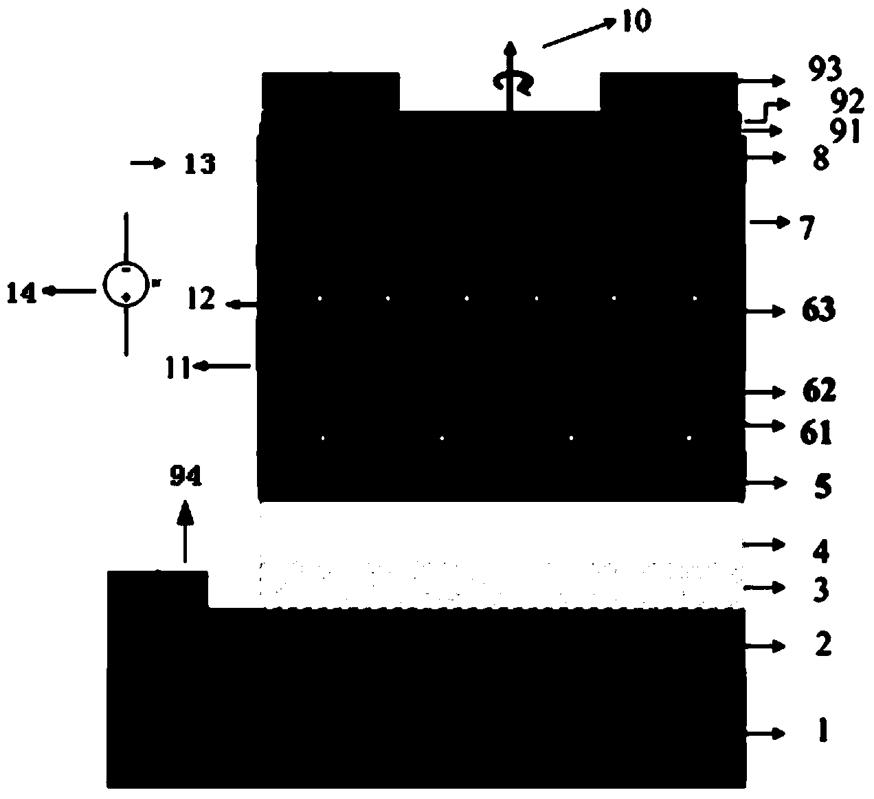
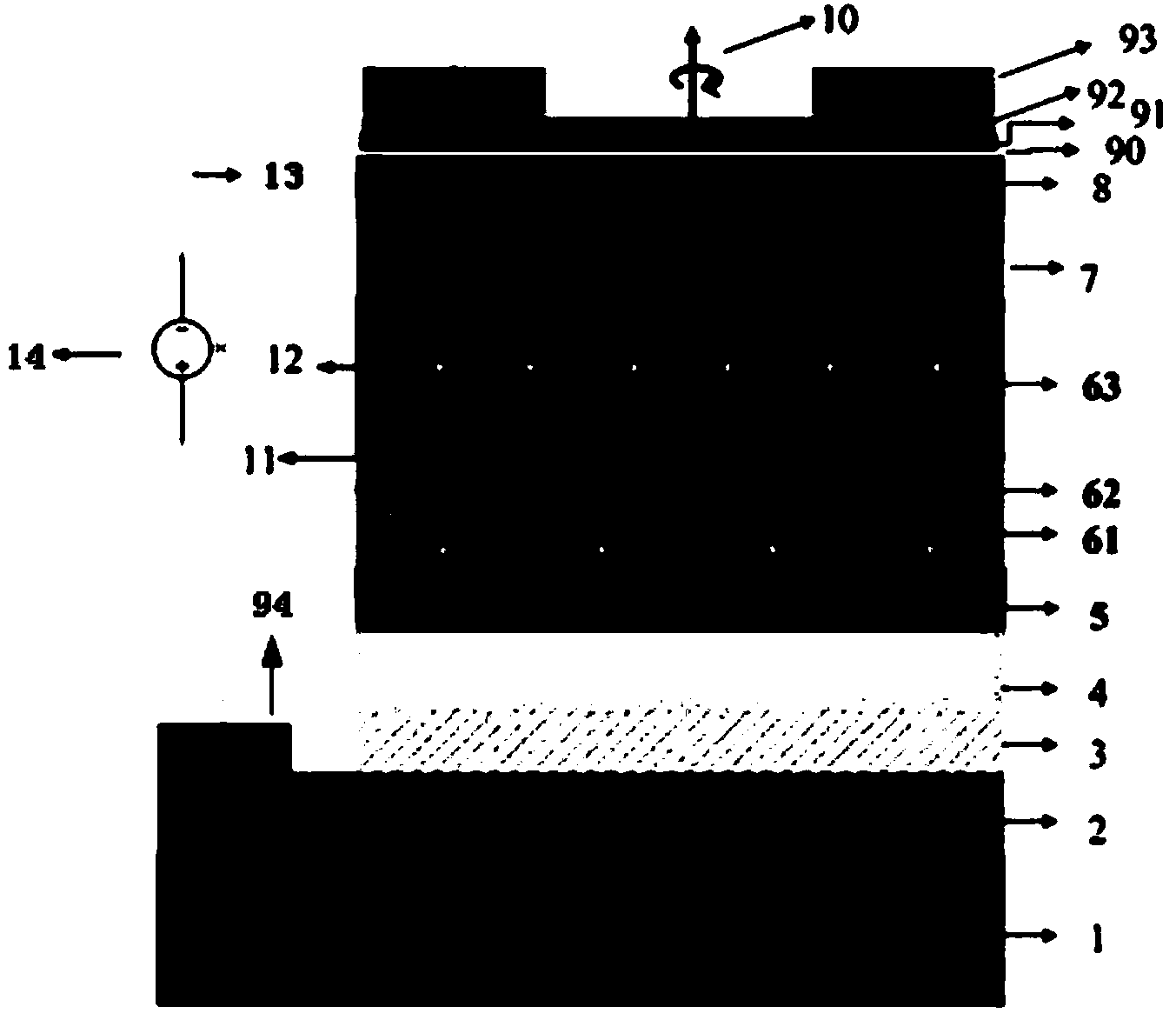
[0038] A spin optoelectronic device described in this embodiment, such as figure 1 and figure 2 As shown, on the substrate layer 1, a p-type buffer layer 2, a barrier layer 3, a first barrier layer 4, a coupled quantum well and a quantum dot structure, a second barrier layer 7, an n-type contact layer 8, and electrodes are grown sequentially. layer, the n-type contact layer 8 forms a spin injection structure with the electrode layer. The electrode layer adopts magnetic metal material, and the magnetic metal material is preferably Fe, Co, Ni and alloys thereof. Wherein, the substrate layer 1 is preferably a p-type substrate.

[0039] The spin optoelectronic device described in this embodiment uses the spin injection structure formed by the n-type contact layer and the electrode layer to transmit the spin-polarized electrons generated in the electrode layer to the coupled quantum well and quantum dot structure, which solves the problem of existing The problem of extremely lo...

Embodiment 2

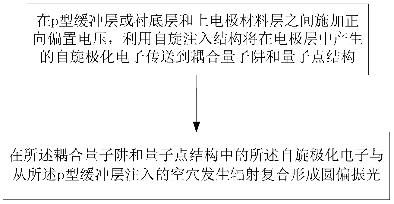
[0049] This embodiment provides a spin injection method based on the spin optoelectronic device described in Embodiment 1, such as image 3 shown, including the following steps:

[0050] S1: Apply a forward bias voltage between the p-type buffer layer or substrate layer and the upper electrode material layer, and use the spin injection structure to transfer the spin-polarized electrons generated in the electrode layer to the coupled quantum well and quantum dot structure ;

[0051] S2: Radiative recombination of the spin-polarized electrons in the coupled quantum well and quantum dot structure with holes injected from the p-type buffer layer to form circularly polarized light.

[0052] Wherein said step S1 specifically includes:

[0053] A forward bias voltage is applied between the p-type buffer layer or substrate layer and the upper electrode material layer through a metal lead, using a magnetic metal-semiconductor (M-S) Schottky junction or a magnetic metal-oxide-semicond...


PUM


Abstract

The invention provides a spin-photoelectron device and a spin injection method of the spin-photoelectron device. According to the method, spin-polarized electrons generated by a magnetic metal layer are conveyed to a coupled quantum well and quantum dot structure through a spin injection structure formed by an n-type contact layer and an electrode layer, an M-S Schottky junction or M-O-S tunnel junction is preferentially selected as the spin injection structure, and therefore the problem of extremely-low spin injection efficiency caused by conductivity mismatching of magnetic metal and a semiconductor in the prior art is solved. The growth sequence of the coupled quantum well and quantum dot structure is as follows: a quantum dot layer, a spacing layer and a quantum well layer, the resonance-tunneling effect between the ground state level of ground-state electrons of a quantum well and the excited state level of quantum dots can be achieved by adjusting components of the quantum dot layer of a semiconductor, components of the quantum well layer of the semiconductor, the thickness of the spacing layer and other parameters, the problem of spin loss caused by energy relaxation is solved, and the spin-polarized electrons can be efficiently injected into the quantum dots of the semiconductor very fast.

Description

technical field [0001] The invention relates to the technical field of semiconductor optoelectronics, in particular to a spin optoelectronic device based on coupled semiconductor quantum wells and quantum dots and a spin injection method thereof. Background technique [0002] Carriers in semiconductor quantum dots are in discrete quantum energy levels due to three-dimensional quantum confinement, which inhibits the Elliott-Yafet and D'yakonov-Perel spin relaxation processes, so semiconductor quantum dots are widely used as efficient information carriers In spin optoelectronic devices and quantum information processing. The spin injection process of spin optoelectronic devices based on semiconductor quantum dot materials is as follows: first, spin-polarized electrons or holes are generated through magnetic electrode materials; then, a bias voltage is applied to the active region containing semiconductor quantum dot materials, and the Spin-polarized electrons or holes are inj...

Claims


Application Information

Patent Timeline
Patent Type & Authority Applications(China)
IPC IPC(8): H01L33/06H01L33/12H01L33/00
CPCH01L33/0012H01L33/06H01L33/14
Inventor 杨晓杰
Owner 苏州强明光电有限公司
Why Eureka
Try Eureka