Method for preparing storage of vertical structure on basis of buried layer

A vertical structure and memory technology, applied in the micro-nano field, can solve the problems of time-consuming and cost-intensive, and achieve the effect of superior process compatibility

Inactive Publication Date: 2014-05-07
INST OF SEMICONDUCTORS - CHINESE ACAD OF SCI
View PDF5 Cites 0 Cited by
  • Summary
  • Abstract
  • Description
  • Claims
  • Application Information

AI Technical Summary

Problems solved by technology

Compared with other processes, the etching and CMP process optimization for new materials is a relatively time-consuming and expensive process, which is also the biggest bottleneck to be faced in the verification of new storage materials

Method used


Image

  • Method for preparing storage of vertical structure on basis of buried layer
  • Method for preparing storage of vertical structure on basis of buried layer
  • Method for preparing storage of vertical structure on basis of buried layer

Examples


Embodiment Construction

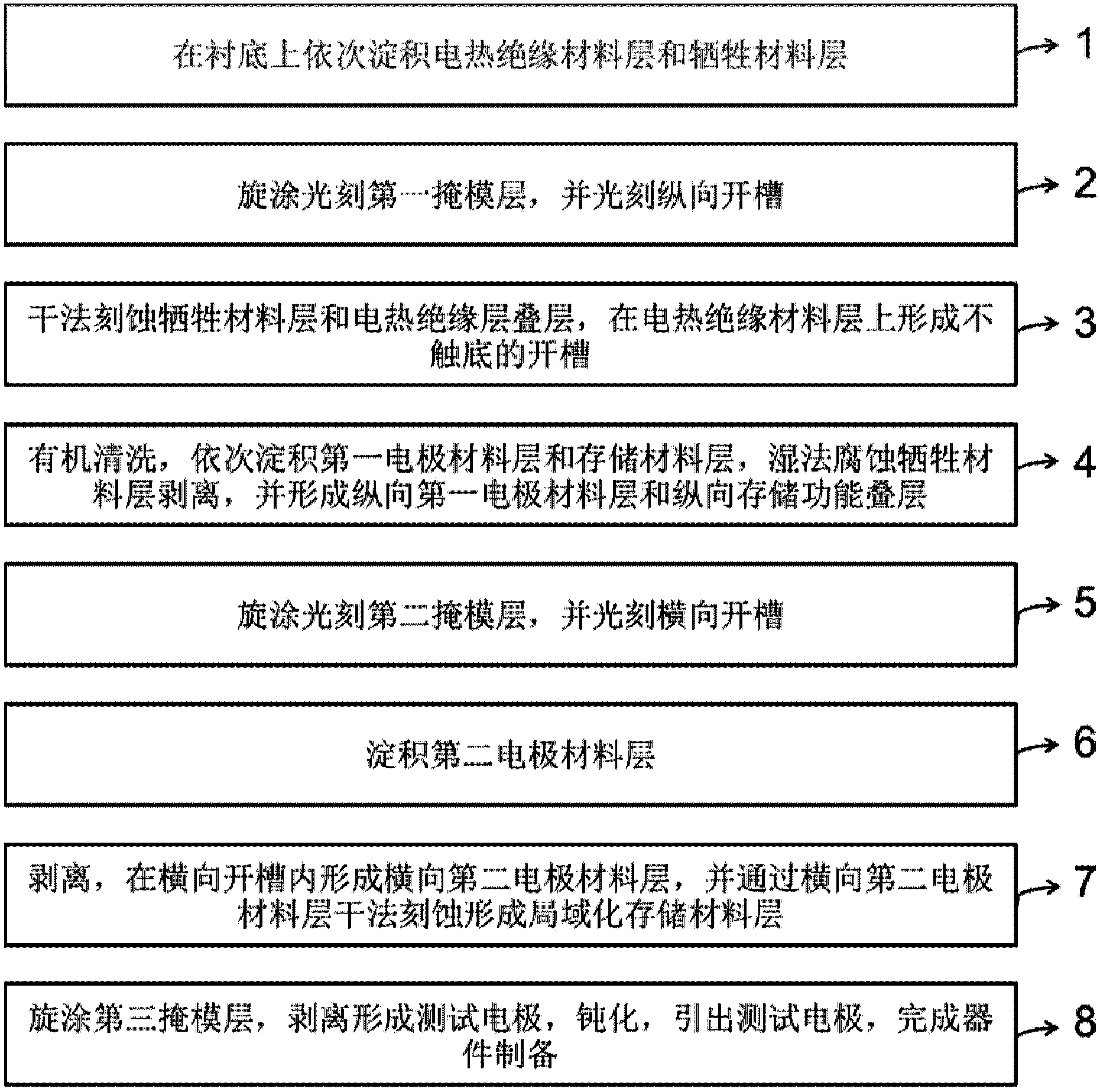
[0020] In order to make the objectives, technical solutions and advantages of the present invention clearer, the present invention will be further described in detail below in conjunction with specific embodiments and with reference to the accompanying drawings.

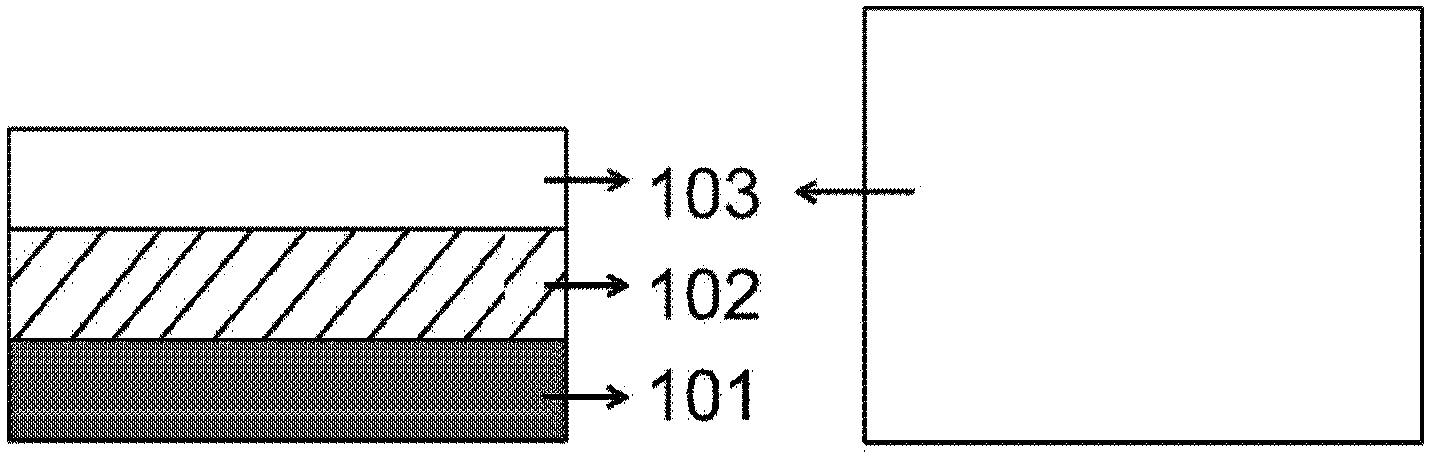
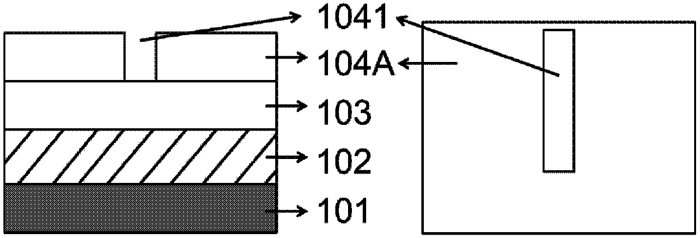
[0021] figure 1 It shows a flow chart of the method for preparing a vertical structure memory based on a buried layer proposed by the present invention. Figure 2A - Figure 2k shows a schematic diagram of the manufacturing process flow of the vertical structure memory based on the buried layer proposed by the present invention. See figure 1 , Figure 2A - As shown in Figure 2k, the present invention provides a method for fabricating a vertical structure memory based on a buried layer. The method includes:

[0022] Step 1: On the substrate 101, sequentially deposit an electrothermal insulating material layer 102 and a sacrificial material layer 103, such as Figure 2A Shown

[0023] The material of the substrate 101 can be s...


PUM


Abstract

The invention discloses a method for preparing a storage of a vertical structure on the basis of a buried layer. According to the method, a bottom electrode is buried, a function material layer is stored, and accordingly good electric heating insulation is achieved, and the situation that a CMP is relied on when a component of a vertical structure is prepared in the prior art is eliminated. According to the method, under the assistance of high-precision linear photoetching means such as electron beam lithography and focused particle beam etching and high-precision thin-film deposition and etching processes, the defects that the development cycle is long, development is difficult, cost is high and adaptability is poor due to development bottlenecks of a CMP technique are solved in development of the vertical structure in the prior art, and the method has great advantages in preparation precision, preparation efficiency, economical performance, compatibility with an existing CMOS process and the like.

Description

Technical field [0001] The invention relates to the field of micro-nano technology, in particular to a method for preparing a vertical structure memory based on a buried layer. Background technique [0002] The accelerated development of high-tech industries and infrastructure service facilities has increasingly higher requirements for fast computing and efficient storage, and the improvement of CPU processing power is increasingly dependent on the speed and power consumption of memory chips, so how to develop efficient storage Become one of the key technologies in urgent need of breakthrough in the future. Phase change memory PCRAM (phase change random access memory) is non-volatile. Compared with most current memories, it has small device size, low power consumption, fast reading speed, anti-irradiation, multi-level storage, and The existing CMOS process is compatible and many other advantages. With a similar device structure, the metal oxide-based resistance memory RRAM has ...

Claims


Application Information

Patent Timeline
Patent Type & Authority Applications(China)
IPC IPC(8): H01L45/00
Inventor 付英春王晓峰杨富华
Owner INST OF SEMICONDUCTORS - CHINESE ACAD OF SCI
Why Eureka
Try Eureka