Device and method for measuring resistance distribution of nano film materials through atomic force microscope

A technology of atomic force microscope and nano-film material, which is applied in the direction of measuring device, scanning probe microscopy, instrument, etc., can solve the problems of large influence of current density distribution, large measurement error, inability to directly and accurately test conductivity, etc., to achieve The effect of low objective requirements, easy operation, and simple device structure

Active Publication Date: 2014-05-14
XI AN JIAOTONG UNIV
View PDF4 Cites 11 Cited by
  • Summary
  • Abstract
  • Description
  • Claims
  • Application Information

AI Technical Summary

Problems solved by technology

This type of method can also be divided into two types according to the different types of electrodes. One is to apply a certain bias voltage between the conductive probe of the conductive atomic force microscope and the substrate of the sample, that is, the probe and the substrate are respectively used as two Electrode, when the probe starts to scan on the surface of the sample, the conductivity distribution of the sample along the thickness direction is analyzed by observing the current change between the probe and the substrate, but in this case the current density distribution inside the sample is affected by Factors such as the shape of the sample and the distribution of the substrate resistance are greatly affected, so the measurement error is relatively large
The other is to make a point electrode on the surface of the sample, add a certain bias voltage between the conductive probe of the atomic force microscope and the point electrode, and observe that when the probe gradually approaches or moves away from the point electrode, the gap between the probe and the point electrode The change of the current is used to test the resistance, but this method can only detect the conductivity of the sample in a very small area around the point electrode along the direction parallel to the sample surface, and the change of the current is also affected by the distance between the probe and the electrode. Because the real distribution of current density is not simply parallel to the sample surface, this method cannot intuitively and accurately test the conductivity difference of the local structure of the material along the direction parallel to the sample surface.

Method used


Image

  • Device and method for measuring resistance distribution of nano film materials through atomic force microscope
  • Device and method for measuring resistance distribution of nano film materials through atomic force microscope
  • Device and method for measuring resistance distribution of nano film materials through atomic force microscope

Examples


Embodiment Construction

[0022] Below in conjunction with accompanying drawing and embodiment the present invention will be described in further detail:

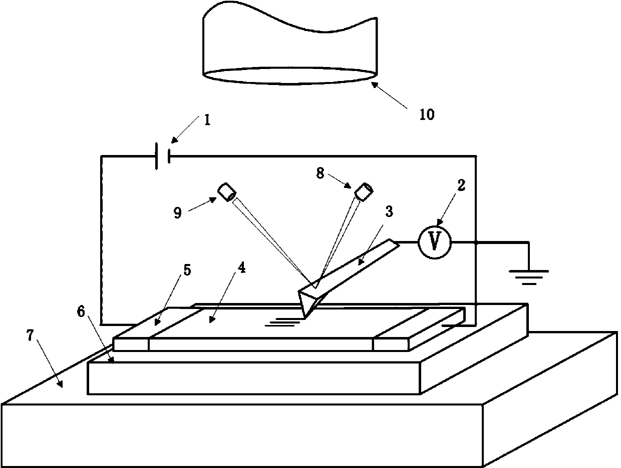
[0023] see figure 1 , the present invention is a device for measuring the resistance distribution of nano-film materials by atomic force microscope, comprising an insulating substrate 6, and a sample 4 to be measured placed on the insulating substrate 6, and rectangular electrodes 5 are respectively arranged on both sides of the sample 4 to be measured, wherein One electrode is connected to the positive pole of the DC power supply 1, the other electrode is connected to the negative pole of the DC power supply 1, the negative pole of the DC power supply 1 is grounded, and the electrode 5 is in contact with the sample 4 to be tested and does not cover the surface of the sample to be tested; to prevent the sample to be tested The insulating substrate 6 of 4 is placed on the piezoelectric displacement loading platform 7 of the atomic force microscope, a...


PUM


Abstract

The invention discloses a device and method for measuring resistance distribution of nano film materials through an atomic force microscope. The system comprises an insulation substrate and a sample to be measured, the sample to be measured is arranged on the insulation substrate, and electrodes are arranged on the two sides of the sample to be measured. The insulation substrate with the sample to be measured is placed on a carrying platform of the atomic force microscope, the tail end of a conductive probe of the atomic force microscope is connected to the positive pole of a voltage meter through a wire, and the negative pole of the voltage meter is grounded; the data output end of the voltage meter is communicated with a computer. According to the device and method, the atomic force microscope is used, a constant direct current parallel to the surface of the sample is exerted on the sample to be measured, the conductive probe of the atomic force microscope is used for measuring earth potentials of all points on the sample, and through calculation of potential difference of adjacent points, resistance distribution conditions of the corresponding two points can be obtained. The device is simple in structure, the objective requirements for the sample are low, measured results are small in error, and materials which are uneven in resistance distribution because of nano structures can be indicated.

Description

technical field [0001] The invention belongs to the technical field of electrical conductivity measurement, and in particular relates to a device and a method for measuring the resistance distribution of nanometer film materials with an atomic force microscope. Background technique [0002] With the development of science and technology, the scale of devices that people can process is getting smaller and smaller, and they are more and more concerned about the influence of nanoscale structures on material properties. As a means of nanoscopic testing, atomic force microscopy has attracted everyone's attention. People try to use it to observe the properties exhibited by nanostructured materials. At present, the use of atomic force microscopy to observe the conductivity of the nanostructure of materials is mainly to judge the conductivity by observing the change of current in the measurement circuit. This type of method can also be divided into two types according to the differ...

Claims


Application Information

Patent Timeline
IPC IPC(8): G01Q60/24
Inventor 刁东风张冬青范雪
Owner XI AN JIAOTONG UNIV
Why Eureka
Try Eureka