How the transistor is formed

A transistor and semiconductor technology, applied in the manufacture of transistors, semiconductor devices, semiconductor/solid-state devices, etc., can solve problems such as poor transistor performance, improve performance, enhance reliability, and avoid excessive reduction.

Active Publication Date: 2016-04-20
SEMICON MFG INT (SHANGHAI) CORP
View PDF6 Cites 0 Cited by
  • Summary
  • Abstract
  • Description
  • Claims
  • Application Information

AI Technical Summary

Problems solved by technology

[0005] However, the transistor performance of the prior art high-K dielectric layer and metal gate structure is not good

Method used


Image

  • How the transistor is formed
  • How the transistor is formed
  • How the transistor is formed

Examples


Embodiment Construction

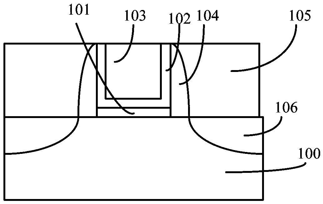
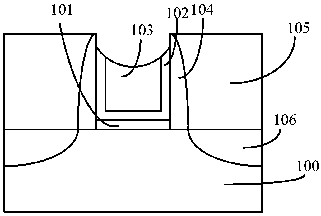
[0032] As mentioned in the background, the performance of the transistor with the high-K dielectric layer and the metal gate structure in the prior art is not good.

[0033] Existing technologies are forming as figure 1 After the shown transistor with high-K dielectric layer and metal gate structure, it is necessary to reduce the height of the work function layer 102 and the metal gate layer 103, so that the surface of the work function layer 102 and the metal gate layer 103 An insulating layer flush with the surface of the dielectric layer 101 is formed, so that the subsequently formed electrical interconnection structure for the transistor can be electrically isolated from the work function layer 102 and the metal gate layer 103 . Specifically, the method for reducing the work function layer 102 and the metal gate layer 103 is: etching the metal gate layer 103 so that the top surface of the metal gate layer 103 is lower than the dielectric layer 101 and the work function lay...


PUM


Abstract

Provided is a transistor forming method which comprises: providing a semiconductor substrate equipped with a dielectric layer on the surface thereof, wherein a first opening passing through the dielectric layer is arranged in the dielectric layer and is composed of a gate structure the surface of which is aligned to the surface of the dielectric layer, the gate structure comprises a gate dielectric layer on the bottom of the first opening, a work function layer covering the gate dielectric layer and the sidewall of the first opening, and a gate electrode layer arranged on the surface of the work function layer and fully filling the first opening, and the work function layer and the gate electrode layer are produced by metal material; etching the work function layer in order that the top surface of the work function layer is lower than that of the dielectric layer; etching the gate electrode layer after etching the work function layer in order that the surface of the gate electrode layer is lower than that of the dielectric layer but higher than that of the work function layer; forming an insulating layer on the surfaces of the gate electrode layer and the work function layer after etching the gate electrode layer in order that the surface of the insulating layer is aligned to the surface of the dielectric layer and the material of the insulating layer is different from the material of the dielectric layer. A formed transistor has excellent performance.

Description

technical field [0001] The invention relates to the technical field of semiconductor manufacturing, in particular to a method for forming a transistor. Background technique [0002] With the rapid development of integrated circuit manufacturing technology, the size of semiconductor devices in integrated circuits, especially MOS (Metal Oxide Semiconductor, metal-oxide-semiconductor) devices, is continuously reduced to meet the miniaturization and integration of integrated circuit development. requirements. In the process of continuous shrinking of the size of MOS transistor devices, the process of using silicon oxide or silicon oxynitride as the gate dielectric layer in the existing process is challenged. Transistors formed with silicon oxide or silicon oxynitride as the gate dielectric layer have some problems, including increased leakage current and diffusion of impurities, which affect the threshold voltage of the transistor and further affect the performance of semicondu...

Claims


Application Information

Patent Timeline
Patent Type & Authority Patents(China)
IPC IPC(8): H01L21/336H01L21/28
CPCH01L21/28017H01L29/4983H01L29/66545H01L29/6656H01L29/66568
Inventor 洪中山
Owner SEMICON MFG INT (SHANGHAI) CORP
Why Eureka
Try Eureka