Fin portion manufacturing method and fin type field effect transistor and manufacturing method thereof

A technology of fin field effect and manufacturing method, applied in semiconductor devices, semiconductor/solid-state device manufacturing, electrical components, etc. The height and shape are difficult to control, etc., to achieve the effect of fast carrier migration speed, increased device density, and easy height

Active Publication Date: 2014-05-21
SEMICON MFG INT (SHANGHAI) CORP +1
View PDF4 Cites 11 Cited by
  • Summary
  • Abstract
  • Description
  • Claims
  • Application Information

AI Technical Summary

Problems solved by technology

[0006] The problem to be solved by the present invention is to propose a new fin manufacturing method, fin field effect transistor and its manufacturing method to improve the existing fin height and shape which are difficult to control, which is not conducive to applying tensile stress or compressive stress to the channel. stress, causing the response speed of the FinFET to be too slow

Method used


Image

  • Fin portion manufacturing method and fin type field effect transistor and manufacturing method thereof
  • Fin portion manufacturing method and fin type field effect transistor and manufacturing method thereof
  • Fin portion manufacturing method and fin type field effect transistor and manufacturing method thereof

Examples


Embodiment Construction

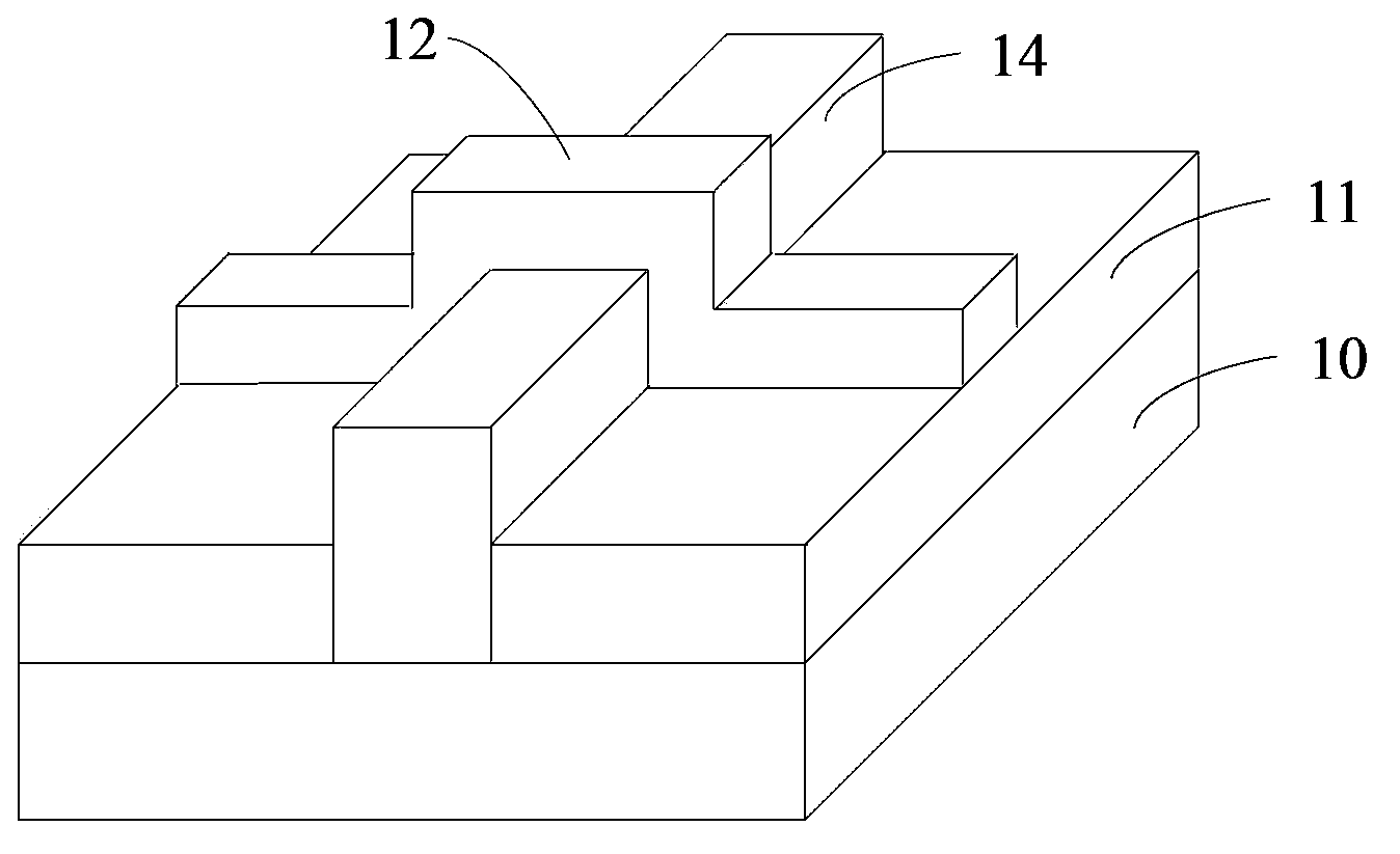
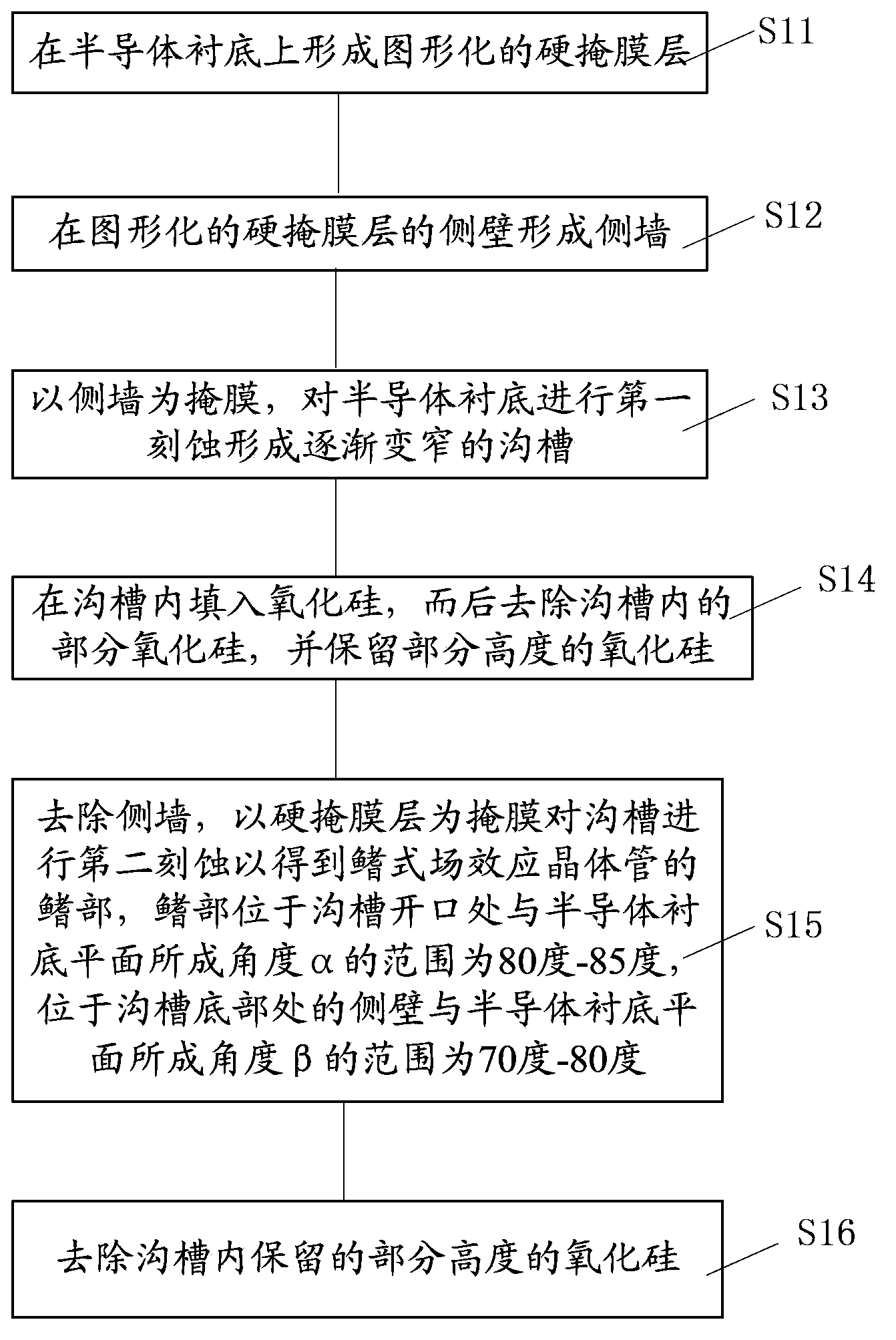
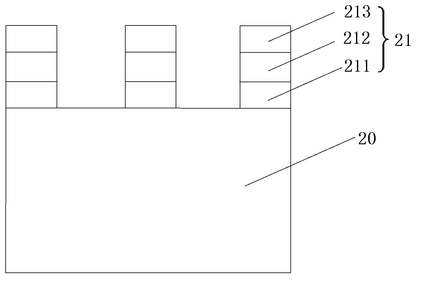
[0038] The height and shape of the fin portion of the fin field effect transistor formed by the prior art manufacturing method is difficult to control, which is not conducive to applying tensile stress or compressive stress to the channel, which will cause the response speed of the fin field effect transistor to be too slow. In view of the above problems, the present invention proposes the following method to form a fin field effect transistor: first, a patterned hard mask layer is formed on a semiconductor substrate; then sidewalls are formed on the sidewalls of the patterned hard mask layer; Then use the sidewall as a mask to first etch the semiconductor substrate to form a gradually narrowing trench; then fill the trench with silicon oxide, remove part after CMP to retain part of the height silicon oxide; then remove the sidewall, and use the hard mask layer as a mask to perform a second etching on the trench to obtain the fin of the fin field effect transistor, and the fin ...


PUM


Abstract

A fin portion manufacturing method comprises forming into an imaging hard mask layer on a semiconductor substrate; forming into a lateral wall on the lateral wall of the imaging hard mask layer; etching a semiconductor substrate for the first time to form into a gradually narrowed groove with the lateral wall serving as a mask; filling silicon oxide into the groove and removing partial silicon oxide inside the groove and reserving partial height of silicon oxide; removing the lateral wall, etching the groove for the second time to obtain the fin portion of the fin type field effect transistor with the hard mask layer serving as the mask. The range of the angle formed between the fin portion lateral wall at the groove opening and the semiconductor substrate plane is 80 to 85 degrees and the range of the angle formed between the fin portion lateral wall at the bottom and the semiconductor substrate is 70 to 80 degrees. The invention also provides a fin type field effect transistor and a manufacturing method thereof based on the fin portion manufacturing method. According to the technical scheme of the fin portion manufacturing method, the height of the fin portion is easy to control and the fin type field effect transistor response time is short.

Description

technical field [0001] The invention relates to the field of semiconductor manufacturing, in particular to a manufacturing method of a fin, a fin field effect transistor and a manufacturing method thereof. Background technique [0002] With the continuous development of semiconductor process technology, as the process node gradually decreases, gate-last (gate-last) process has been widely used to obtain an ideal threshold voltage and improve device performance. However, when the feature size (CD, Critical Dimension) of the device is further reduced, even if the gate-last process is adopted, the structure of the conventional MOS field effect transistor can no longer meet the requirements for device performance. Widespread concern. [0003] Fin field effect transistor (Fin FET) is a common multi-gate device, figure 1 A schematic diagram of a three-dimensional structure of a fin field effect transistor in the prior art is shown. Such as figure 1 As shown, it includes: a sem...

Claims


Application Information

Patent Timeline
Patent Type & Authority Applications(China)
IPC IPC(8): H01L21/28H01L21/336H01L29/78H01L29/423
CPCH01L21/308H01L21/3088H01L29/66795H01L29/785H01L29/7851
Inventor 隋运奇张海洋王新鹏
Owner SEMICON MFG INT (SHANGHAI) CORP
Why Eureka
Try Eureka