

Circuit board packaging structure and manufacturing method thereof
A technology of packaging structure and manufacturing method, which is applied in the direction of assembling printed circuits with electrical components, printed circuits connected with non-printed electrical components, etc., can solve the problem of damage to the adhesive layer and epoxy resin covering the substrate, affecting the inductance value, cost increase etc.
- Summary
- Abstract
- Description
- Claims
- Application Information
AI Technical Summary
Problems solved by technology
Method used
Image

Examples
Embodiment Construction
[0075] A number of embodiments of the present invention will be disclosed below with the accompanying drawings. For the sake of clarity, many practical details will be described together in the following description. It should be understood, however, that these practical details should not be used to limit the invention. That is, in some embodiments of the present invention, these practical details are unnecessary. In addition, for the sake of simplifying the drawings, some conventional structures and elements will be shown in a simple and schematic way in the drawings.
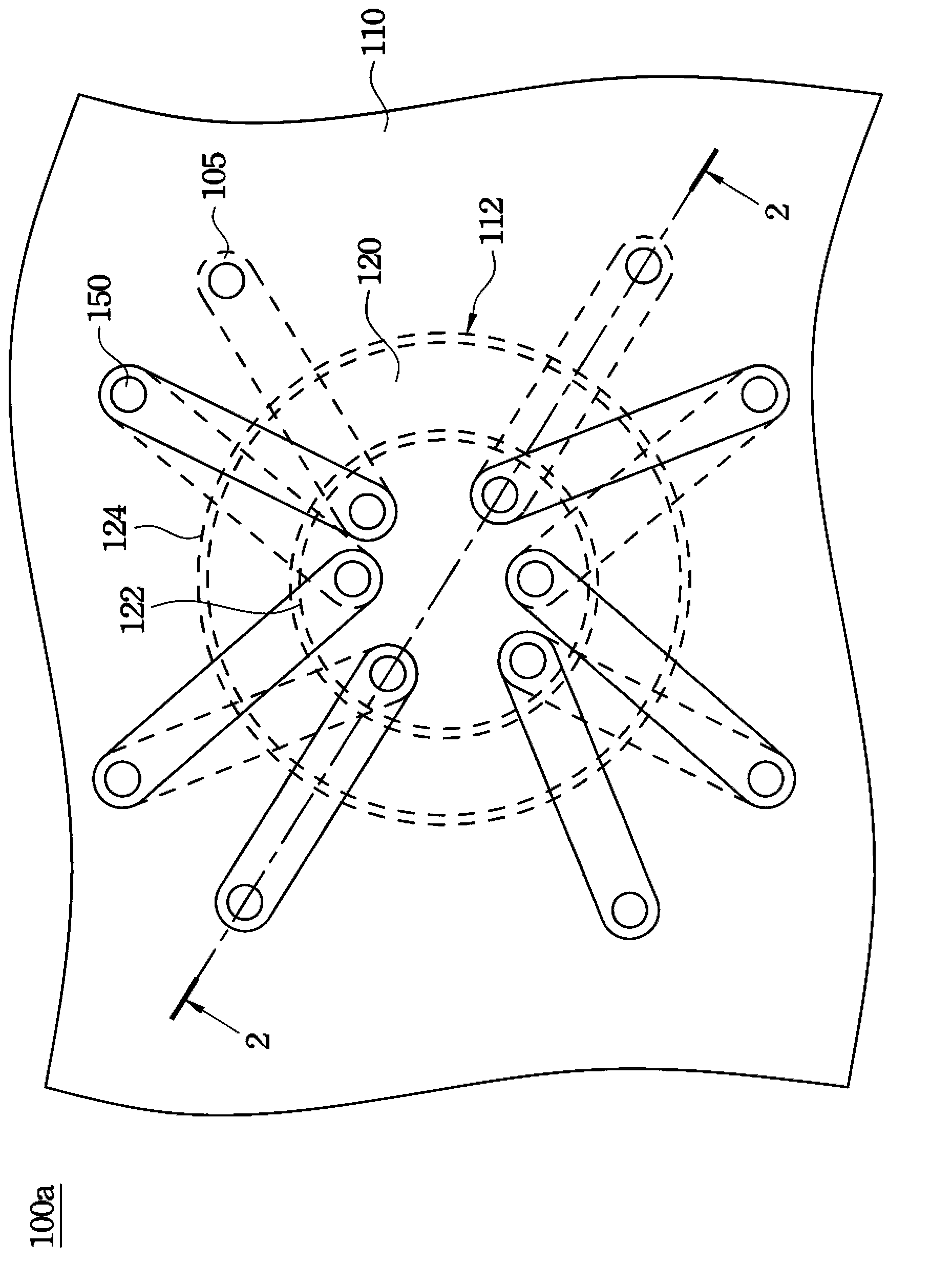
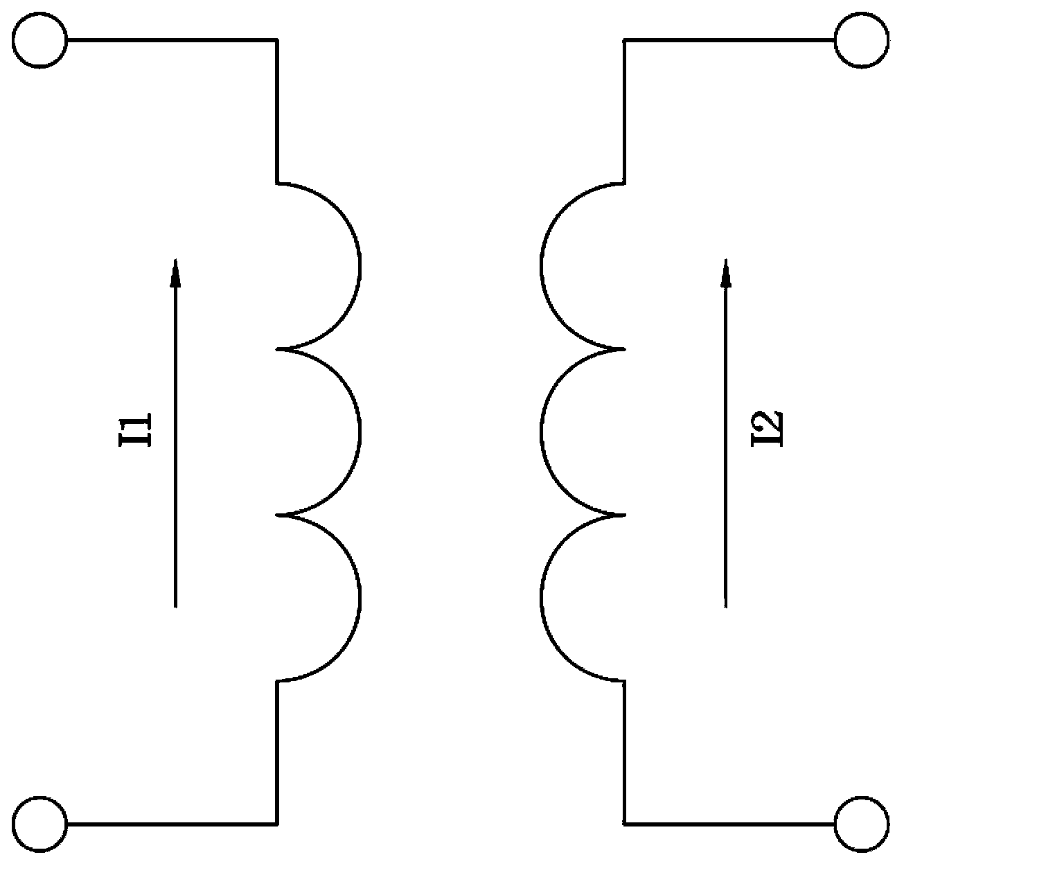
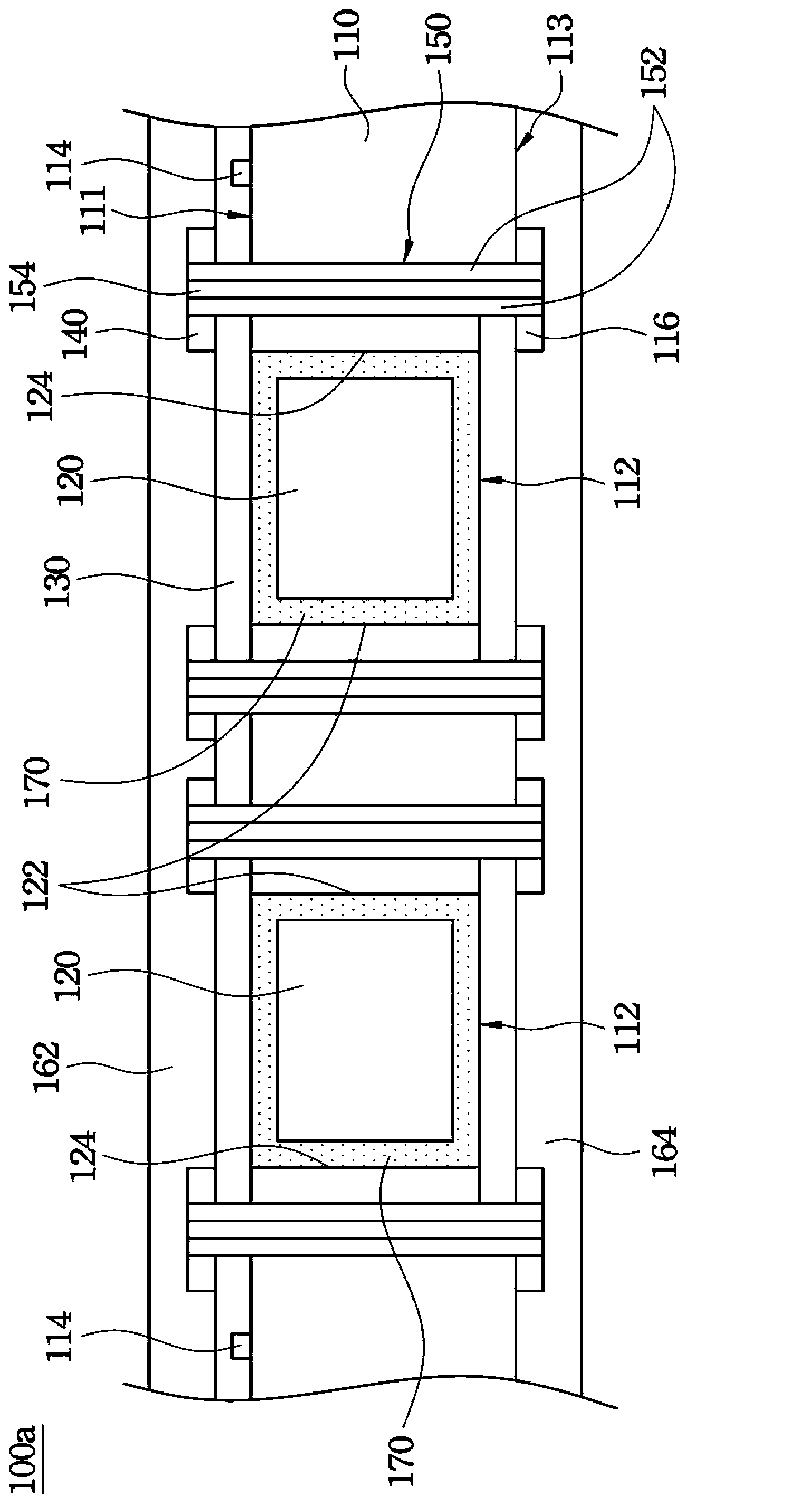
[0076] Figure 1A A top view of a circuit board packaging structure 100a according to an embodiment of the present invention is shown. Figure 1B draw Figure 1A The schematic diagram of the equivalent circuit. see also Figure 1A and Figure 1B , the circuit board packaging structure 100a has a plurality of conductive channels 150 and a plurality of circuits 105, wherein the configuration of the circuits ...
PUM
 Abstract
Description
Claims
Application Information