Three-dimensional display panel and manufacturing method thereof, and three-dimensional display device

A three-dimensional display and panel technology, applied in optics, instruments, electrical components, etc., can solve problems such as film damage, complex production process, and impact on display quality, and achieve the effect of reducing production costs, simplifying production processes, and avoiding poor display.

Inactive Publication Date: 2014-05-28
BOE TECH GRP CO LTD
View PDF8 Cites 24 Cited by
  • Summary
  • Abstract
  • Description
  • Claims
  • Application Information

AI Technical Summary

Problems solved by technology

[0005] When manufacturing the 3D display device with the above-mentioned structure, the OLED device 01 and the liquid crystal grating 02 are respectively manufactured first, and then the base substrate 101 of the OLED device 01 and the upper substrate 201 of the liquid crystal grating 02 are bonded together by laminating technology. The process is more complicated
Moreover, in the process of laminating the base substrate 101 of the OLED device 01 and the upper substrate 201 of the liquid crystal grating 02, it is necessary to press the cover glass 102 in the OLED device 01, which may damage the layers of the OLED device 01. cause damage that affects display quality

Method used


Image

  • Three-dimensional display panel and manufacturing method thereof, and three-dimensional display device
  • Three-dimensional display panel and manufacturing method thereof, and three-dimensional display device
  • Three-dimensional display panel and manufacturing method thereof, and three-dimensional display device

Examples


Embodiment Construction

[0031] The specific implementation manners of the 3D display panel provided by the embodiments of the present invention, its manufacturing method and the 3D display device will be described in detail below with reference to the accompanying drawings.

[0032] The shape and thickness of each film layer in the accompanying drawings do not reflect their true proportions, and the purpose is only to illustrate the content of the present invention.

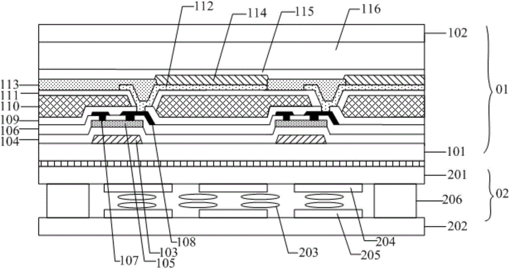
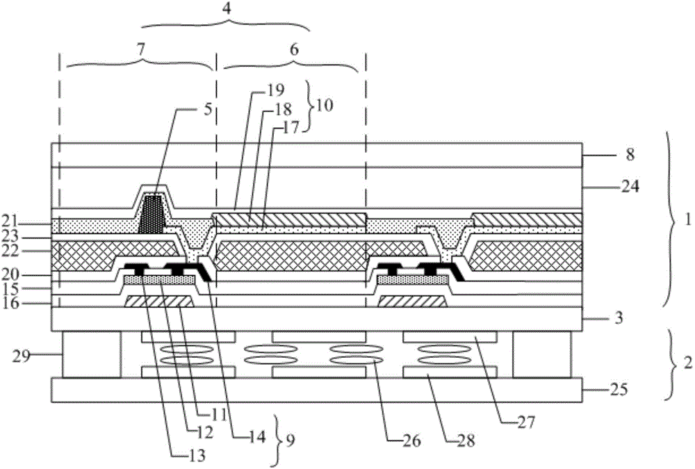
[0033] A three-dimensional display panel provided by an embodiment of the present invention, such as Figure 2a and Figure 2b As shown, it includes: an organic electroluminescent display device 1, and a liquid crystal grating 2 located on the light emitting side of the organic electroluminescent display device 1;

[0034] The organic electroluminescent display device 1 and the liquid crystal grating 2 share the first base substrate 3 between the organic electroluminescent display device 1 and the liquid crystal grating 2 .

[0035] I...


PUM


Abstract

The invention discloses a three-dimensional display panel and a manufacturing method thereof, and a three-dimensional display device. The three-dimensional display panel comprises an organic electroluminescent display device and a liquid crystal raster arranged at the light-emitting side of the organic electroluminescent display device. Because the organic electroluminescent display device and the liquid crystal raster share one substrate, so that one substrate is saved and thus the production cost is lowered; and the thickness of the three-dimensional display panel is reduced. Moreover, the process of contact of the organic electroluminescent display device with the liquid crystal raster is saved; the manufacturing process is simplified; and a problem of poor display caused by damages of all film layers in the organic electroluminescent display device can be avoided during the contact process.

Description

technical field [0001] The invention relates to the field of display technology, in particular to a three-dimensional display panel, a manufacturing method thereof and a three-dimensional display device. Background technique [0002] At present, three-dimensional (Three-Dimensional, 3D) display technology has attracted much attention. It can make the picture three-dimensional and realistic. Superimposed and regenerated to form images with stereoscopic effects. [0003] Among existing display devices, Organic Electroluminescent Display (OLED) has gradually become the mainstream in the display field due to its low power consumption, high color saturation, and wide viewing angle. [0004] Existing OLED-based 3D display devices are made by directly laminating OLED devices and liquid crystal gratings, such as figure 1 As shown, the OLED device 01 includes a base substrate 101 and a cover glass 102 facing each other. On the base substrate 101, a gate 103, a gate insulating layer...

Claims


Application Information

Patent Timeline
Patent Type & Authority Applications(China)
IPC IPC(8): H01L27/32G02B27/22H04N13/30
CPCH04N13/00H04N13/30H10K59/50H10K59/00
Inventor 舒适齐永莲曹占锋周春苗姚琪
Owner BOE TECH GRP CO LTD
Why Eureka
Try Eureka