CCD detecting device

A technology of testing equipment and pulse timing, which is applied in the direction of measuring equipment, measuring electricity, and measuring electrical variables, etc., can solve the problems of the CCD vertical timing driving circuit, such as specific problems, large workload and hardware consumption, and lack of versatility, so as to reduce Effects of hardware consumption, reduction of hardware consumption, and efficiency improvement

Active Publication Date: 2014-06-04
THE 44TH INST OF CHINA ELECTRONICS TECH GROUP CORP
View PDF6 Cites 6 Cited by
  • Summary
  • Abstract
  • Description
  • Claims
  • Application Information

AI Technical Summary

Problems solved by technology

[0002] In the prior art, when the CCD is tested, the conventional design idea is: for each kind of CCD, a set of driving timing and driving circuit are separately designed, and the typical CCD vertical timing driving circuit is such as the vertical driving circuit introduced by Kadak Company (KODAK KAI-0340 CCD IMAGE SENSORIMAGER EVALUATION BOARDUSERS MANUAL, REVISION 1.0 APRIL 19, 2004), this circuit is aimed at the working characteristics of the clock phase Φvi pulse in the imaging area of ​​CCD devices with different structures requiring a long time in "H" or "L", the vertical drive circuit Correspondingly, two circuit structures of "H" clamp or "L" clamp are also designed, but there are differences in the structure of the two circuits of "H" clamp and "L" clamp, resulting in the vertical drive circuit of the finished product It can only adapt to a specific type of CCD drive requirements, and cannot be used for other purposes. This vertical drive circuit is not universal, so in production, it is necessary to redesign the drive circuit separately for different types of CCDs. The workload and The hardware consumption is large, and it is very cumbersome, and the production cost is high
[0003] The inventor had previously proposed a patent application (hereinafter referred to as the reference) entitled "CCD driving timing generation method and its driving timing generating device" (application number: CN201310353387). The core of this technology is: based on the same hardware device, Different timing pulses can be obtained by changing the control parameters, thereby generating corresponding CCD drive signals. The hardware involved includes the control parameter adjustment device (that is, the terminal equipment in the reference), the timing pulse generation device (that is, the reference in the reference Processing chip) and CCD drive signal generation device (that is, CCD vertical timing drive circuit); the aforementioned invention patent application proposes a brand-new design idea for the CCD test device, but does not propose a specific implementation method for the specific CCD vertical timing drive circuit

Method used


Image

  • CCD detecting device
  • CCD detecting device

Examples


Embodiment Construction

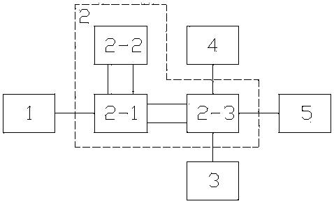
[0013] A kind of CCD testing device, it is characterized in that: comprise pulse sequence signal generation module 1, CCD vertical sequence drive circuit 2, high level DC source 3 and low level DC source 4; In described pulse sequence signal generation module 1 at least include A terminal device for human-machine dialogue and a processing chip. The operator inputs various preset control parameters into the processing chip through the terminal device, and the processing chip generates corresponding pulse timing signals according to different control parameters; Under the control of the signal, the CCD vertical timing drive circuit 2 can perform time-sharing gate processing on the high-level DC source 3 and the low-level DC source 4, so as to obtain the CCD drive signal corresponding to the pulse timing signal.

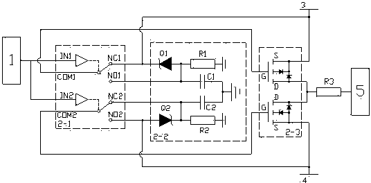
[0014] Further, the CCD vertical timing drive circuit is composed of a switch module 2-1, a voltage stabilizing circuit 2-2 and a power amplitude amplification circuit 2...


PUM


Abstract

A CCD detecting device is characterized in that a pulse time sequence signal generating module, a CCD vertical time sequence driving circuit, a high-level direct-current source and a low-level direct-current source are included, the pulse time sequence signal generating module at least comprises a terminal device for man-machine interaction and a processing chip, operators input various preset control parameters into the processing chip through the terminal device, the processing chip generates corresponding pulse time sequence signals according to different control parameters, under the control effect of the pulse time sequence signals, the CCD vertical time sequence driving circuit can carry out time-sharing gating processing on the high-level direct-current source and the low-level direct-current source, and accordingly CCD driving signals corresponding to the pulse time sequence signals are obtained. The CCD detecting device has the advantages that one detecting circuit set can meet the detecting requirements of different types of CCDs, hardware consumption during a detecting process is lowered, trivial work that in the prior art, driving circuits need to be independently designed for different types of CCDs is avoided, and detecting working efficiency is indirectly improved.

Description

technical field [0001] The invention relates to a device for CCD testing, in particular to a CCD testing device. Background technique [0002] In the prior art, when the CCD is tested, the conventional design idea is: for each kind of CCD, a set of driving timing and driving circuit are separately designed, and the typical CCD vertical timing driving circuit is such as the vertical driving circuit introduced by Kadak Company (KODAK KAI-0340 CCD IMAGE SENSORIMAGER EVALUATION BOARDUSERS MANUAL, REVISION 1.0 APRIL 19, 2004), this circuit is aimed at the working characteristics of the clock phase Φvi pulse in the imaging area of ​​CCD devices with different structures requiring a long time in "H" or "L", the vertical drive circuit Correspondingly, two circuit structures of "H" clamp or "L" clamp are also designed, but there are differences in the structure of the two circuits of "H" clamp and "L" clamp, resulting in the vertical drive circuit of the finished product It can ...

Claims


Application Information

Patent Timeline
Patent Type & Authority Applications(China)
IPC IPC(8): G01R31/00
Inventor 周建勇熊路袁世顺张婷婷唐遵烈彭秀华
Owner THE 44TH INST OF CHINA ELECTRONICS TECH GROUP CORP
Why Eureka
Try Eureka