Light-emitting-diode chip

A technology of light-emitting diodes and chips, applied in electrical components, circuits, semiconductor devices, etc., can solve the problems of low light output and reduce the light-emitting area of ​​light-emitting diode chips, and achieve the effect of increasing the light-emitting area, improving the light output and small area.

Inactive Publication Date: 2014-06-04
ZHANJING TECH SHENZHEN +1
View PDF3 Cites 8 Cited by
  • Summary
  • Abstract
  • Description
  • Claims
  • Application Information

AI Technical Summary

Problems solved by technology

However, in order to make the bonding wires planted on the LED chip, the metal electrode pad must have a certain area, for example, the area of ​​the metal electrode pad is usually 50um×50um, in this way, the metal electrode pad must block part of the light, thus Reduce the light-emitting area of ​​the LED chip, resulting in low light output

Method used


Image

  • Light-emitting-diode chip
  • Light-emitting-diode chip
  • Light-emitting-diode chip

Examples


Embodiment Construction

[0017] The present invention will be further described in detail below in conjunction with the accompanying drawings.

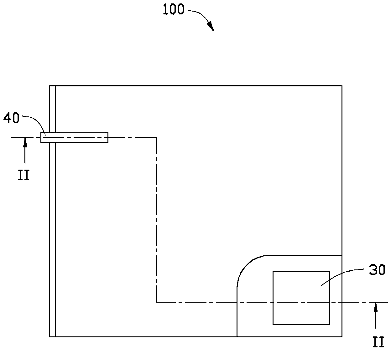
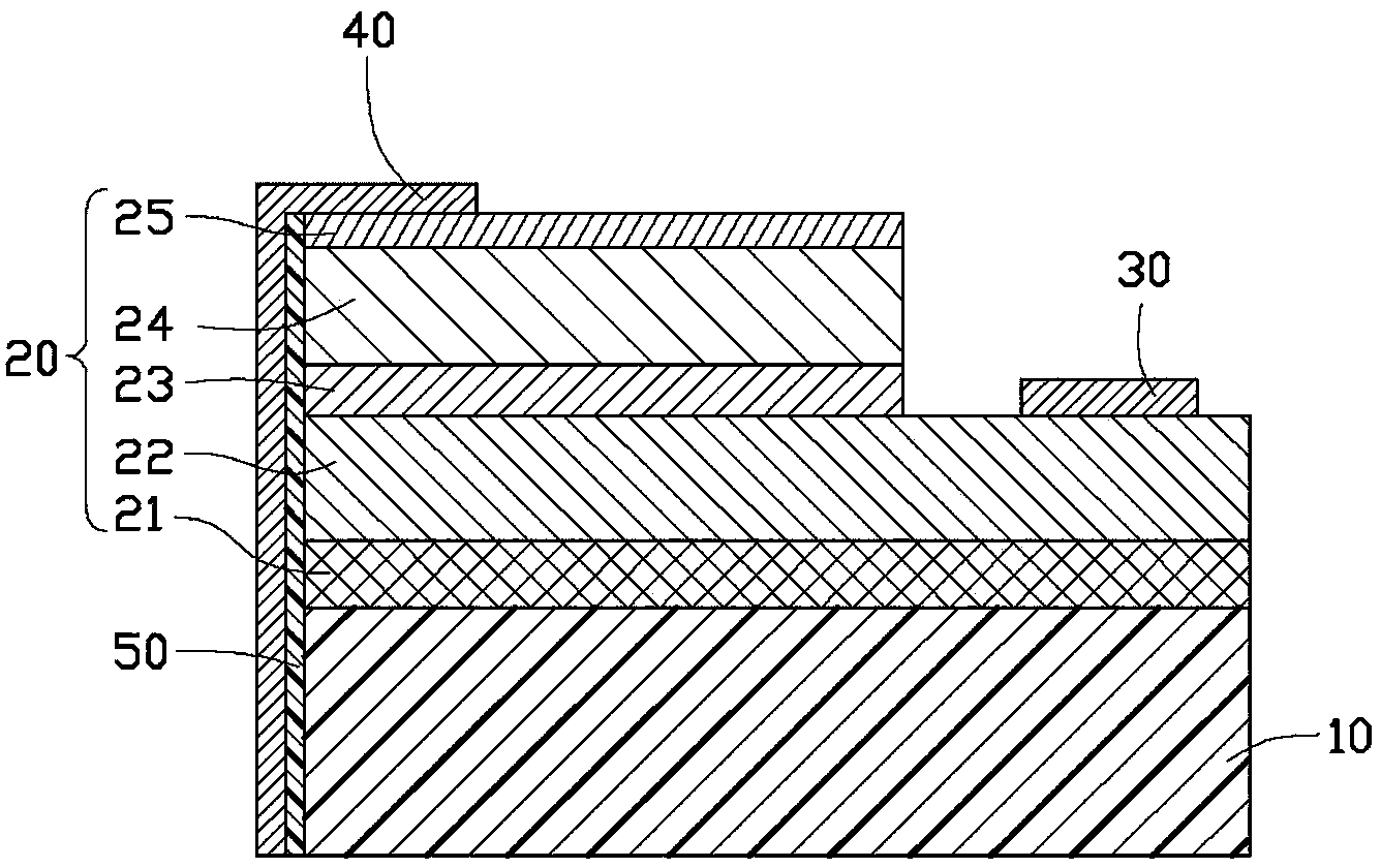
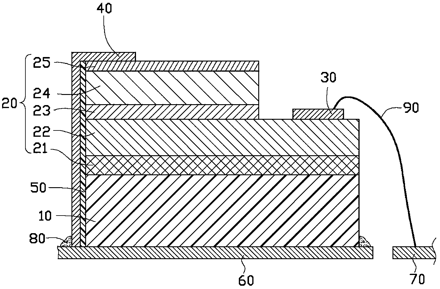
[0018] see figure 1 as well as figure 2 A light emitting diode chip 100 provided in the first embodiment of the present invention includes a substrate 10 , a semiconductor structure 20 formed on the substrate 10 , and an N-type electrode 30 and a P-type electrode 40 formed on the semiconductor structure 20 .

[0019] The substrate 10, as a substrate for growing semiconductor structures, can be sapphire (Sapphire), silicon carbide (SiC), silicon (Si), gallium arsenide (GaAs), lithium metaaluminate (LiAlO2), magnesium oxide (MgO), Zinc oxide (ZnO), gallium nitride (GaN), aluminum nitride (AlO), or indium nitride (InN), etc.

[0020] The semiconductor structure 20 includes a buffer layer 21 , an N-type semiconductor layer 22 , an active layer 23 , a P-type semiconductor layer 24 and a conductive layer 25 grown sequentially on the substrate 10 . The buffer la...


PUM


Abstract

Disclosed is a light-emitting-diode chip which includes a substrate, a semiconductor structure formed on the substrate and two electrodes which are formed on the semiconductor structure and mutually spaced. The semiconductor structure is provided with two exposed semiconductor layers, wherein one electrode is formed on the upper surface of one semiconductor layer and the other electrode is formed on the upper surface of the other semiconductor structure. At least one of the two electrodes extend in a bent manner from the upper surface of a corresponding semiconductor layer to the side face of the semiconductor structure and is electrically connected with an external electrode through a conductive glue. The electrodes of the light-emitting-diode chip do not need to be connected by gold wires so that compared with traditional metal electrode pads, the electrodes of the light-emitting-diode chip do not need to be provided with areas for gold wire welding and thus the areas of the electrodes can be significantly small so that the light-blocking areas of the electrodes are reduced, the light-emitting area of the light-emitting-diode chip is increased and the light exiting quantity is improved.

Description

technical field [0001] The invention relates to a light emitting diode chip. Background technique [0002] The LED (light-emitting diode, Light-emitting diode) industry is one of the most watched industries in recent years. Mercury has the advantages of environmental benefits, so it is considered to be the best light source for the new generation of green energy-saving lighting. [0003] In the prior art, a P-type metal electrode pad and an N-type metal electrode pad are generally provided on the LED chip, and then gold wires are used to electrically connect the metal electrode pad of the LED chip to the welding pad of the substrate. However, in order to make the bonding wires planted on the LED chip, the metal electrode pad must have a certain area, for example, the area of ​​the metal electrode pad is usually 50um×50um, in this way, the metal electrode pad must block part of the light, thus The light-emitting area of ​​the light-emitting diode chip is reduced, resulting ...

Claims


Application Information

Patent Timeline
Patent Type & Authority Applications(China)
IPC IPC(8): H01L33/38
CPCH01L33/385
Inventor 沈佳辉洪梓健
Owner ZHANJING TECH SHENZHEN
Why Eureka
Try Eureka