A method for measuring the electronic gain multiple of a charge-coupled device

A charge-coupled device and electronic gain technology, applied in the testing of a single semiconductor device, etc., can solve the problems of inaccurate measurement results, non-consideration of non-linear characteristics of sense amplifiers, read-out noise errors, and measurement errors. The effect of improving measurement accuracy

Inactive Publication Date: 2016-06-08
INST OF OPTICS & ELECTRONICS - CHINESE ACAD OF SCI
View PDF5 Cites 0 Cited by
  • Summary
  • Abstract
  • Description
  • Claims
  • Application Information

AI Technical Summary

Problems solved by technology

This method does not take into account the nonlinear characteristics of the CCD sense amplifier, the CCD front-end preprocessing circuit and the measurement error introduced by the noise generated by these parts, resulting in inaccurate measurement results
[0006] Another measurement method based on analog signal quantity is consistent with the measurement principle based on digital quantity, except that the observation object is changed to the analog signal quantity output by the CCD: use an oscilloscope to directly observe the analog signal quantity amplitude of the CCD with or without gain The magnitude of the electronic gain multiple can be used to shield the non-linearity introduced by the CCD front-end preprocessing circuit and the circuit noise generated. Compared with the first method, it has been improved, but it still does not take into account the non-linear characteristics of the sense amplifier of the EMCCD. and errors introduced by read noise

Method used


Image

  • A method for measuring the electronic gain multiple of a charge-coupled device
  • A method for measuring the electronic gain multiple of a charge-coupled device
  • A method for measuring the electronic gain multiple of a charge-coupled device

Examples


Embodiment Construction

[0018] In order to make the object, technical solution and advantages of the present invention clearer, the present invention will be described in further detail below in conjunction with specific embodiments and with reference to the accompanying drawings.

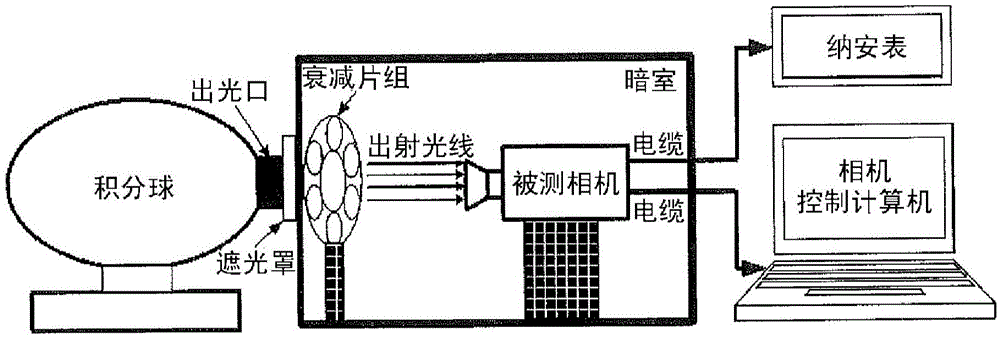
[0019] figure 1 It shows a method for measuring the electronic gain multiple of a charge-coupled device of the present invention, which uses an electronic multiplying charge-coupled device composed of an integrating sphere, a light shield, an attenuation film group, a measured camera, a darkroom, a camera control computer, and a nanoampere meter. The electronic gain multiplier measuring device measures the electronic multiplication charge coupled device.

[0020] The present invention is aimed at the embodiment of charge-coupled device (CCD), and described charge-coupled device is the area array charge-coupled device, those skilled in the art can realize the electronic gain related to any area array charge-coupled device ...


PUM


Abstract

The invention discloses a method for measuring the electron gain factor of a charge coupled device. The method comprises the following steps: S1, acquiring and absorbing signal electrons stored on a floating grid capacitor to form reset grid weak current when a reset metal-oxide semiconductor tube of a read amplifier of the charge coupled device is conducted; S2, detecting the reset grid weak current of the reset metal-oxide semiconductor tube on the read amplifier through a nano-ammeter; S3, calculating the sum of average electrons of each pixel on the floating grid capacitor according to the reset grid weak current to detect the electron gain factor of a detected camera. By adopting the method, the problem of increase of the measuring error of the electron gain factor due to non-linear feature of the read amplifier of the charge coupled device and produced read noise is solved. The method is very suitable for measuring the electron gain factor of the charge coupled device in an electron gain calibrating process.

Description

technical field [0001] The invention belongs to the field of low-light imaging, and relates to a method for measuring the electron gain multiple of an electron multiplying charge-coupled device. Background technique [0002] Electron Multiplying Charge Coupled Device (EMCCD) is a new technology that has emerged in the field of CCD image sensors in the past ten years. The high-voltage electric field can amplify the signal electrons by more than 1000 times before the signal electrons are converted into a signal voltage by the sense amplifier, thereby suppressing the post-gain noise introduced by the sense amplifier and circuit noise, and obtaining very high sensitivity, especially suitable for micro light imaging. Compared with the traditional charge-coupled device (CCD) with an image intensifier, its structure and volume are greatly simplified, and it has great advantages in some applications that are sensitive to weight and volume. [0003] Electron multiplier The measurem...

Claims


Application Information

Patent Timeline
Patent Type & Authority Patents(China)
IPC IPC(8): G01R31/26
Inventor 王明富任国强刘非周向东马文礼
Owner INST OF OPTICS & ELECTRONICS - CHINESE ACAD OF SCI
Why Eureka
Try Eureka