An etching process and device for improving sidewall streaks

A streak and process technology, applied in the field of etching process and its devices, can solve the problems of polymer sidewall streaks, high DC bias, and polymer weight, and achieve the effect of improving the streaks of through holes

Active Publication Date: 2016-10-19
ADVANCED MICRO FAB EQUIP INC CHINA
View PDF5 Cites 0 Cited by
  • Summary
  • Abstract
  • Description
  • Claims
  • Application Information

AI Technical Summary

Problems solved by technology

However, we found that even if only 60MHz is used to etch BARC and TEOS (or DARC), the DC bias generated by it is also very high, and the surface and sidewall of the photoresist are seriously damaged during the etching process.
Moreover, at around 60MHz, the concentration of the plasma is high, and the polymer produced is also heavy, which is difficult to control, and the uneven deposition of the polymer also causes serious sidewall streaks.

Method used


Image

  • An etching process and device for improving sidewall streaks
  • An etching process and device for improving sidewall streaks
  • An etching process and device for improving sidewall streaks

Examples


Embodiment 1

[0076] Using the etching process and device for improving sidewall streaks of the present invention to etch the bottom dielectric isolation layer includes the following specific steps:

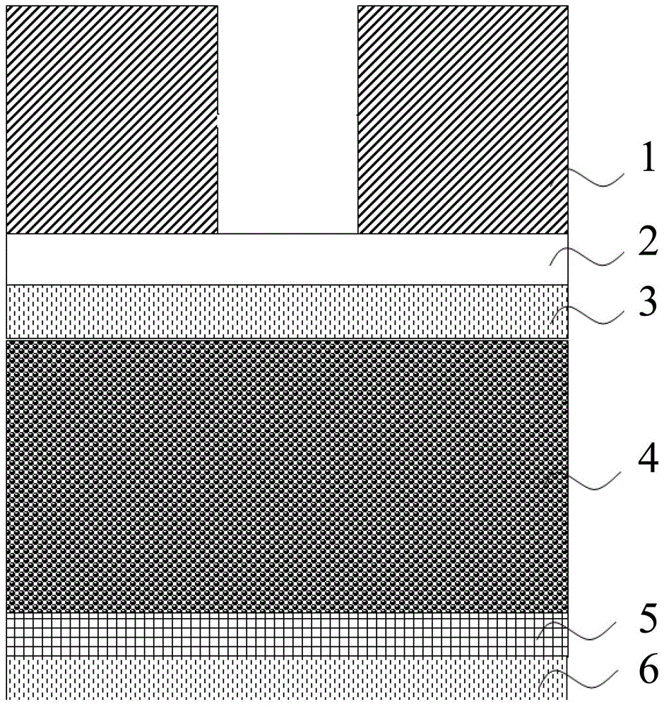
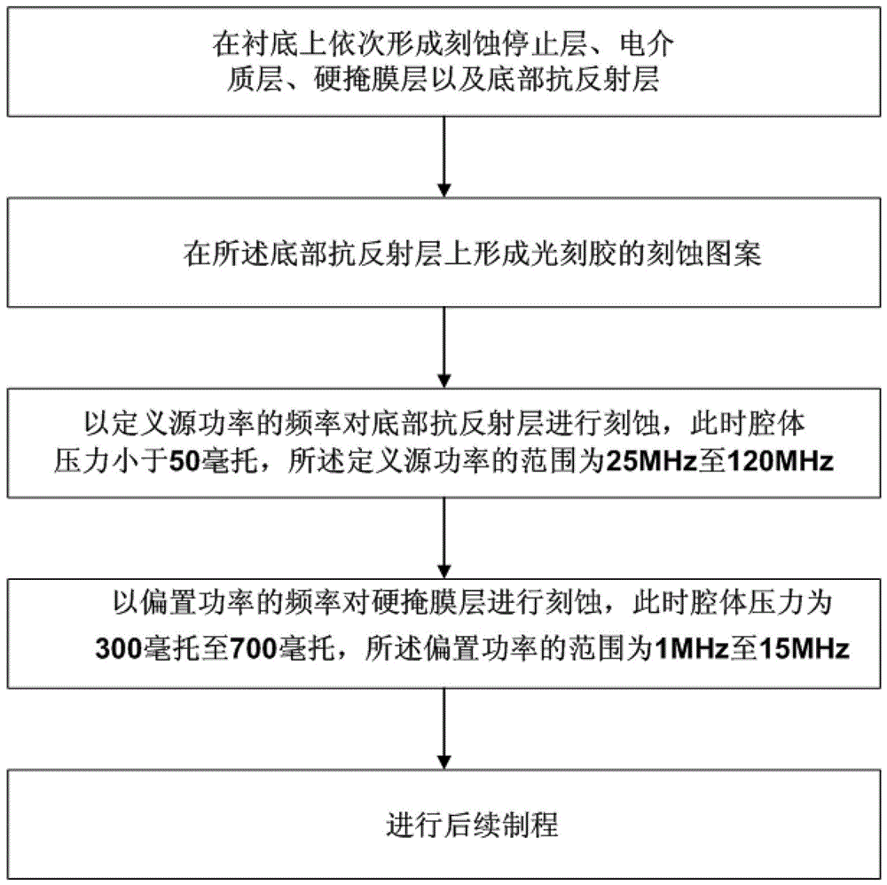
[0077] The substrate is placed on the pedestal in the plasma reaction chamber, and an etching stop layer, a dielectric layer, a hard mask layer and a bottom anti-reflection layer are sequentially formed on the substrate.

[0078] An etching pattern of photoresist is formed on the bottom anti-reflection layer.

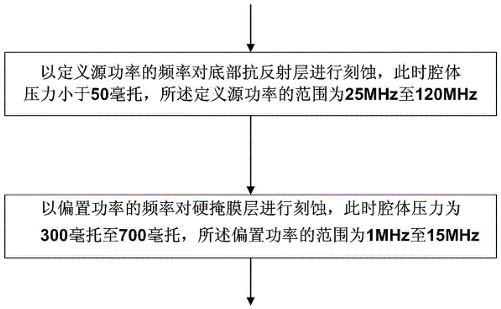
[0079] The plasma generator in the plasma reaction chamber etches the bottom anti-reflection layer at a frequency that defines the source power. At this time, the chamber pressure is 45 mTorr, and the mixed gas introduced during the etching of the bottom anti-reflection layer includes: N 2 and CO 2 The mixed gas, the defined source power is 60MHz.

[0080] Then the plasma generator etches the hard mask layer at the frequency of the bias power, and the cavity pressure is 600 millitorr ...

Embodiment 2

[0084] Using the etching process and device for improving sidewall streaks of the present invention to etch the bottom dielectric isolation layer includes the following specific steps:

[0085] The substrate is placed on the pedestal in the plasma reaction chamber, and an etching stop layer, a dielectric layer, a hard mask layer and a bottom anti-reflection layer are sequentially formed on the substrate.

[0086] An etching pattern of photoresist is formed on the bottom anti-reflection layer.

[0087] The plasma generator in the plasma reaction chamber etches the bottom anti-reflection layer at a frequency that defines the source power. At this time, the chamber pressure is 40 mTorr, and the mixed gas introduced during the etching of the bottom anti-reflection layer includes: N 2 and O 2 The mixed gas, the defined source power is 70MHz.

[0088] Then the plasma generator etches the hard mask layer at the frequency of the bias power. At this time, the chamber pressure is 500 ...

Embodiment 3

[0092] Using the etching process and device for improving sidewall streaks of the present invention to etch the bottom dielectric isolation layer includes the following specific steps:

[0093] The substrate is placed on the pedestal in the plasma reaction chamber, and an etching stop layer, a dielectric layer, a hard mask layer and a bottom anti-reflection layer are sequentially formed on the substrate.

[0094] An etching pattern of photoresist is formed on the bottom anti-reflection layer.

[0095] The plasma generator in the plasma reaction chamber etches the bottom anti-reflection layer at a frequency that defines the source power. At this time, the chamber pressure is 35 mTorr, and the mixed gas introduced during the etching of the bottom anti-reflection layer includes: N 2 and CO 2 The mixed gas, the defined source power is 65MHz.

[0096] Then the plasma generator etches the hard mask layer at the frequency of the bias power. At this time, the chamber pressure is 550...


PUM


Abstract

The invention provides an etching method and device for improving side wall streaks. The method is applied to a substrate, wherein a bottom anti-reflection layer and a hard mask layer are formed on the surface of the substrate. The method includes the following steps that the bottom anti-reflection layer is etched at the frequency of define source power, and at the time, cavity pressure is lower than 50 millitorrs; the hard mask layer is etched at the frequency of bias power, and at the time, the cavity pressure ranges from 300 millitorrs to 700 millitorrs; the define source power ranges from 25 MHz to 120 MHz, and the bias power ranges from 1 MHz to 15 MHz. When a bottom dielectric isolation layer is etched by means of the etching method and device for improving the side wall streaks, the rough streaks of the side faces of photoresists do not extend downward, so that damage to the surface and the side wall of a polymer layer is avoided. Compared with the prior art, by means of the method and device, the surface and the side wall of the etched polymer layer are not rough and do not have the streaks, and the streaks of through holes are greatly improved.

Description

technical field [0001] The invention relates to an etching process and a device for improving sidewall streaks, in particular to an etching process and a device for respectively etching a bottom anti-reflection layer and a hard mask layer through two different etching processes. Background technique [0002] Dry etching is a technique that uses plasma to etch thin films. When the gas exists in the form of plasma, it has two characteristics: on the one hand, the chemical activity of these gases in the plasma is much stronger than that under normal conditions. React with the material to achieve the purpose of etching and removal; on the other hand, the electric field can also be used to guide and accelerate the plasma, so that it has a certain energy. When it bombards the surface of the etched object, it will be etched The atoms of the object material are knocked out, so as to achieve the purpose of etching by physical energy transfer. Therefore, dry etching is the result of...

Claims


Application Information

Patent Timeline
Patent Type & Authority Patents(China)
IPC IPC(8): H01L21/311
CPCH01J37/32H01L21/31116H01L21/67069
Inventor 刘志强王兆祥杜若昕黄智林
Owner ADVANCED MICRO FAB EQUIP INC CHINA
Why Eureka
Try Eureka