Machining method for circuit board drilling

A processing method and circuit board technology, which is applied in multilayer circuit manufacturing, printed circuit components, electrical connection printed components, etc., can solve problems such as difficulty in ensuring the yield rate of circuit boards, and achieve reduced product defect rate and good product performance , to avoid the effect of circuit board damage

Inactive Publication Date: 2014-06-11
SHENNAN CIRCUITS
View PDF6 Cites 9 Cited by
  • Summary
  • Abstract
  • Description
  • Claims
  • Application Information

AI Technical Summary

Problems solved by technology

[0003] The purpose of the embodiments of the present invention is to provide a processing method for drilling holes in circuit boards, aimin...

Method used


Image

  • Machining method for circuit board drilling
  • Machining method for circuit board drilling
  • Machining method for circuit board drilling

Examples


Embodiment Construction

[0018] In order to make the object, technical solution and advantages of the present invention clearer, the present invention will be further described in detail below in conjunction with the accompanying drawings and embodiments. It should be understood that the specific embodiments described here are only used to explain the present invention, not to limit the present invention.

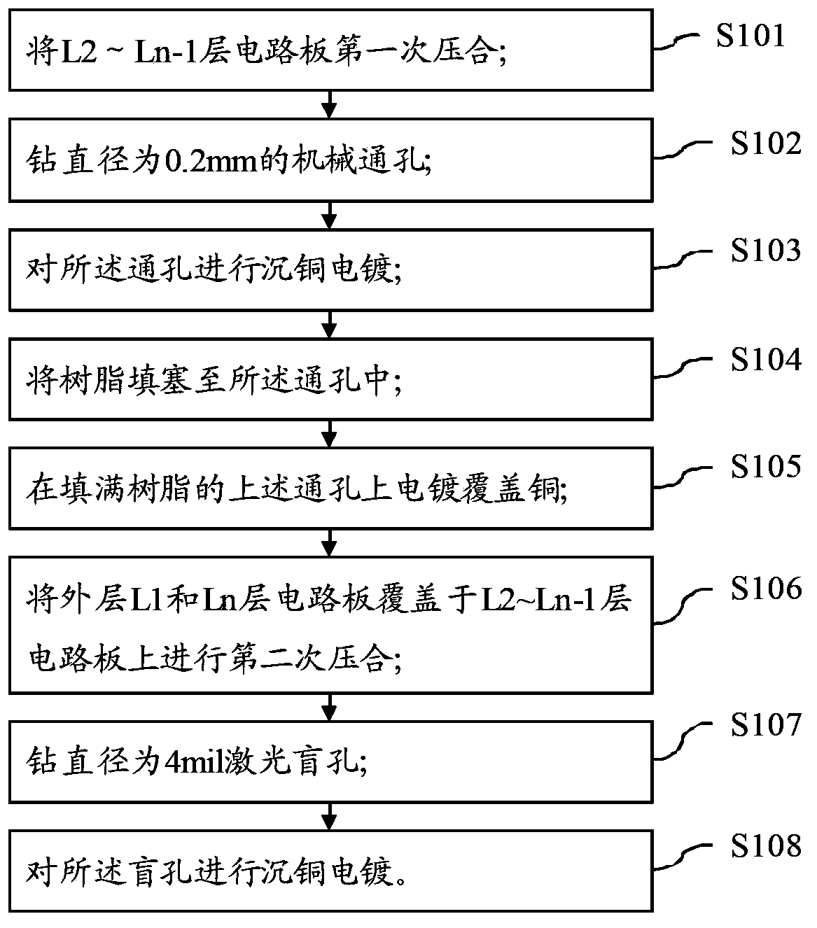
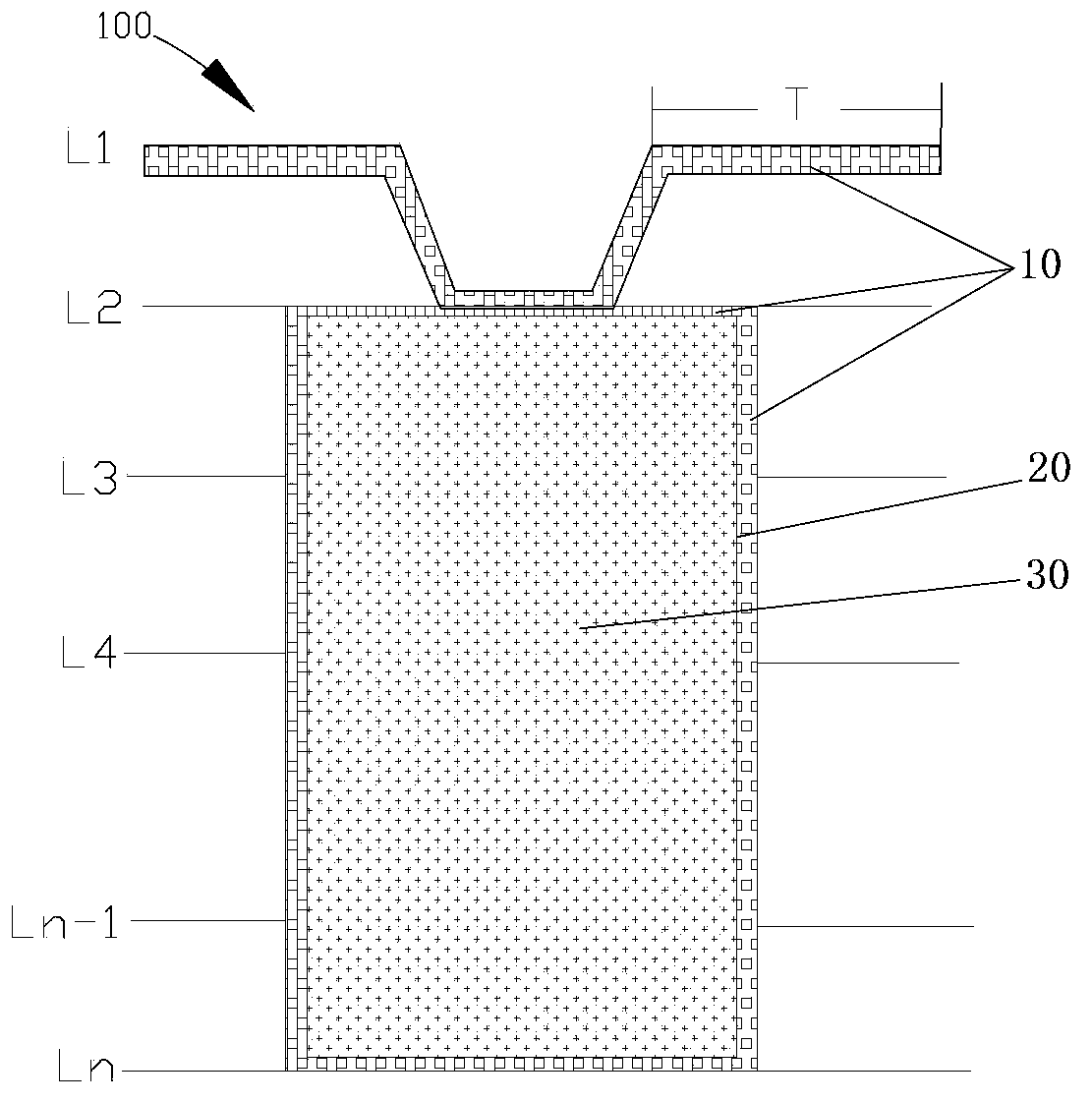
[0019] Please also refer to Figure 1 to Figure 3 , the circuit board drilling processing method provided by the embodiment of the present invention mainly uses the combination of electroplating copper processing method and high density interconnection processing method (High Density Interconnection, referred to as HDI) to realize drilling and routing on the circuit board 100. Wire.

[0020] In this embodiment, the circuit board 100 is a ball grid array circuit board (Ball Grid Array PCB, BGA for short), and the size of the circuit board 100 is 0.6 mm.

[0021] This processing method specifically...


PUM

PropertyMeasurementUnit
Sizeaaaaaaaaaa

Abstract

The invention relates to the field of circuit board processing, and provides a machining method for circuit board drilling. The method aims to solve the problem that due to wiring of a ball grid array (BGA) PCB with the diameter of 0.6 mm, the yield of a circuit board is difficult to guarantee. The machining method for circuit board drilling includes the following steps that primary bonding is carried out on L2 to Ln-1 layers of circuit boards; mechanical through holes with the diameter of 0.2 mm are drilled; copper electroplating is carried out on the through holes; the through holes are filled with resin; copper is electroplated and covers the through holes filled with the resin; the L1 layer of circuit board and the Ln layer of circuit board cover the L2-Ln-1 layers of the circuit boards for secondary bonding; laser blind holes with the diameter of 4 mil are drilled; copper electroplating is carried out on the blind holes. The invention further provides a circuit board formed through the method. By means of combination of the electroless copper technology processing method and HDI, drilling in the BGA PCB is achieved, so that conducting and wiring functions are achieved, good use performance of products is guaranteed, and the defective rate of the products is lowered.

Description

technical field [0001] The invention belongs to the field of circuit board processing, and in particular relates to a processing method for drilling holes in a circuit board. Background technique [0002] With the development of the printed circuit board industry, the circuit board is becoming more and more refined, and the lines arranged in the circuit board are getting thinner and the spacing is getting smaller and smaller. Even in the circuit board design of the 0.6mm ball grid array structure circuit board (Ball Grid Array PCB, BGA for short). Using traditional processing methods to perform drilling and pattern processing on such BGA circuit boards is difficult to process, and it is difficult to guarantee the yield of BGA circuit boards. Therefore, this has become a problem that the industry needs to solve. Contents of the invention [0003] The purpose of the embodiments of the present invention is to provide a processing method for drilling holes in circuit boards, ...

Claims


Application Information

Patent Timeline
IPC IPC(8): H05K3/42H05K3/46H05K1/11
Inventor 刘海龙耿宪国罗斌
Owner SHENNAN CIRCUITS
Why Eureka
Try Eureka