Thin film evaporation coating apparatus, and method for making OLED display device

A display device and thin film technology, which is applied in vacuum evaporation plating, sputtering plating, ion implantation plating, etc., can solve the problems of limited shape and structure, low strength, reducing the effective use area of ​​the substrate, etc., so as to improve the effective use Area and strength improvement effect

Inactive Publication Date: 2014-06-18
SHANGHAI TIANMA MICRO ELECTRONICS CO LTD
View PDF2 Cites 14 Cited by
  • Summary
  • Abstract
  • Description
  • Claims
  • Application Information

AI Technical Summary

Problems solved by technology

Thin film materials cannot be evaporated on the substrate in this area, thus reducing the effective use area of ​​the substrate
In addition, the design of the outline structure of the frame 40 is limited. Since a part of the groove 41 is provided on the plan view surface, the strength of the frame 40 is also low, and it is easy to deform after 30 meshes of the mask.

Method used


Image

  • Thin film evaporation coating apparatus, and method for making OLED display device
  • Thin film evaporation coating apparatus, and method for making OLED display device
  • Thin film evaporation coating apparatus, and method for making OLED display device

Examples


Embodiment 1

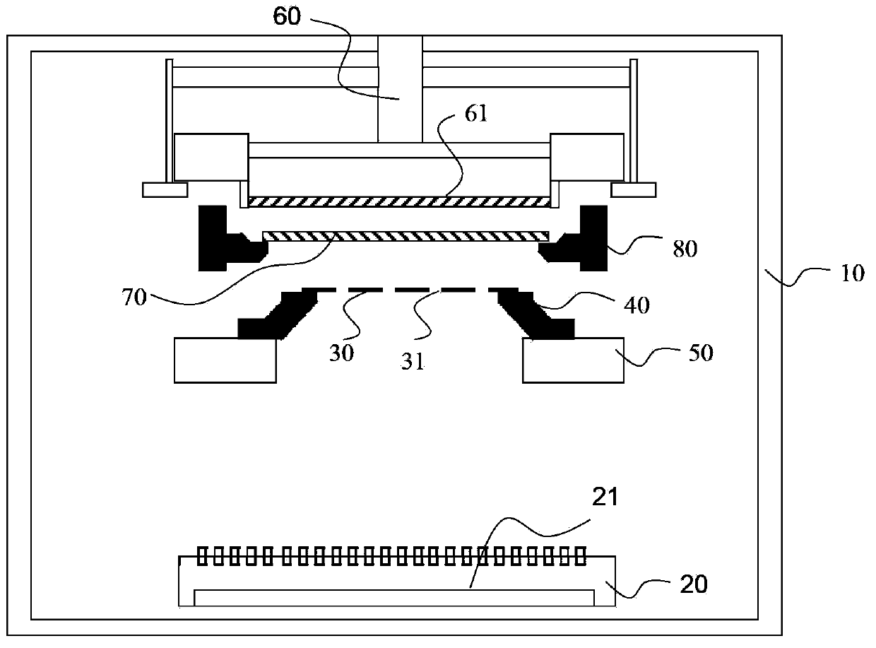
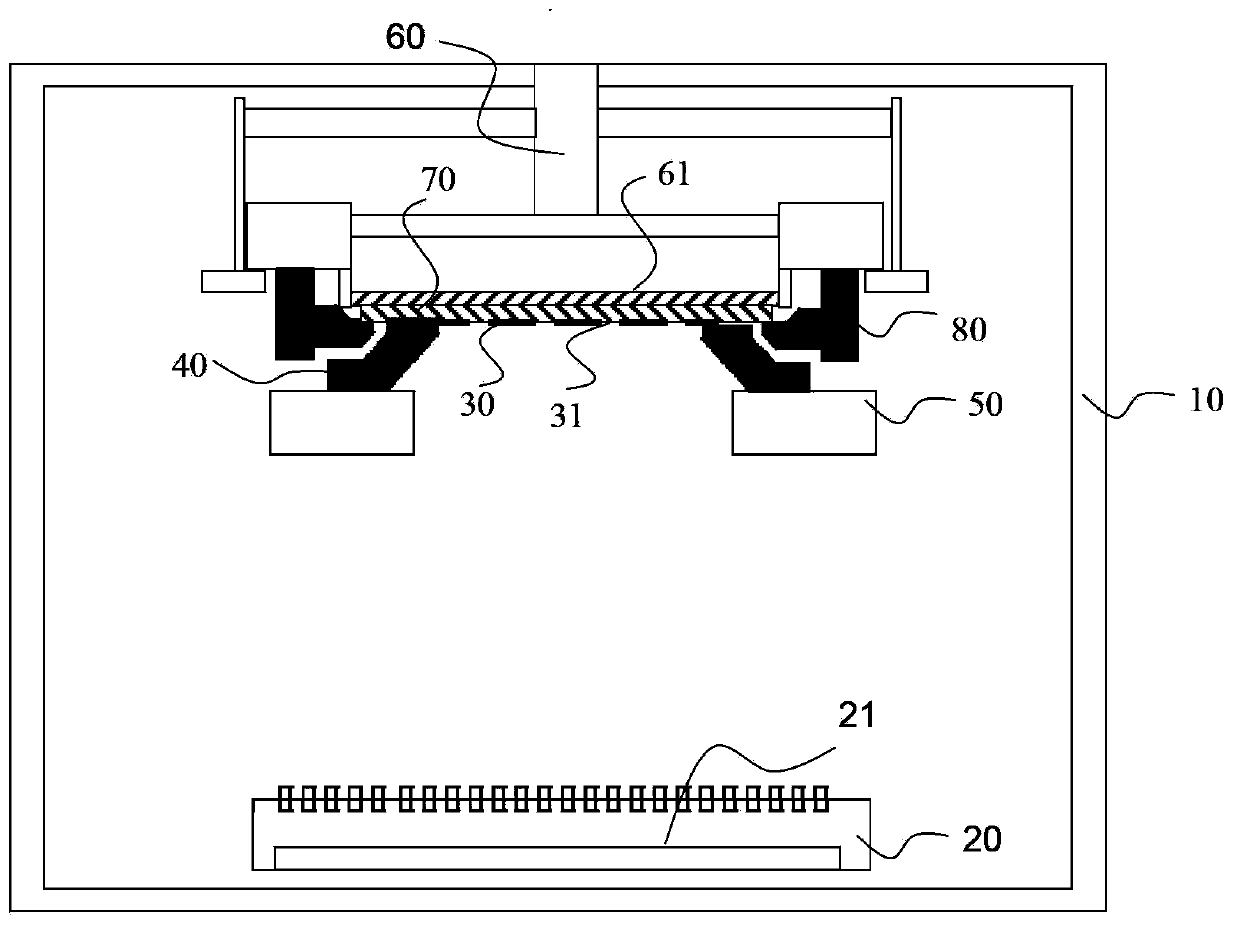
[0048] The schematic diagram of the cross-sectional structure of the thin film evaporation equipment in this embodiment is as follows Figure 4 , Figure 5 shown. The thin film evaporation equipment includes: a cavity 110, and the cavity 110 is provided with: an evaporation source accommodating part 120 near the bottom of the cavity 110, a mask plate 130, a frame 140, a platform 150, a pressing plate 161, and a pressing plate 161 that can drive the pressing plate 161 to move up and down The moving mechanism 160, the substrate receiving fixture 180 for receiving the substrate 170, the electrostatic thin film layer 190 and the protective layer 200. The moving mechanism 160 is close to the top of the cavity 110 and above the evaporation source accommodating part 120, the pressing plate 161 is arranged on the lower side of the moving mechanism 160 and is directly connected with the moving mechanism 160; the substrate receiving fixture 180 is arranged between the pressing plate 16...

Embodiment 2

[0057] Based on the thin film evaporation equipment disclosed in Embodiment 1, this embodiment discloses a method for manufacturing an OLED display device using the thin film evaporation equipment. The flow chart of the method is as follows Figure 7 shown, including:

[0058] Step S101: setting the evaporation source 121 on the evaporation source accommodating part 120;

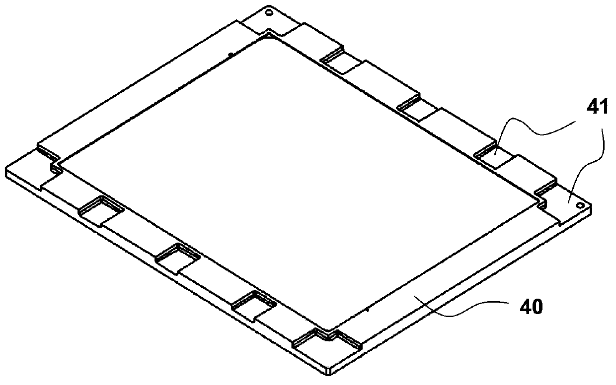
[0059] Step S102: setting the mask plate 130 on the frame 140, the mask plate 130 is provided with several openings 131, the lower edge of the mask plate 130 is supported by the frame 140, and the surface of the frame 140 carrying the mask plate 130 extends out of the mask plate 130;

[0060] In this embodiment, the frame 140 is preferably a hollowed-out closed structure with four sections of hexahedrons vertically connected to each other, and the inner side of each section of hexahedron is an oblique plane at an acute angle with the horizontal plane, and the upper surface and outer side of each secti...


PUM


Abstract

The invention provides a thin film evaporation coating apparatus, and a method for making an OLED display device by utilizing the apparatus. The apparatus comprises: a cavity, wherein an evaporation source accommodation part used for accommodating an evaporation source is arranged in the cavity; a press plate and a movable mechanism driving the press plate to move up and down; a substrate carrying clamp used for carrying a substrate; a frame used for bearing a mask plate; and an electrostatic thin film layer arranged on the lower surface of the press plate. The electrostatic thin film layer enables the substrate to be evenly adsorbed on the press plate in an electrostatic adsorption manner and to be separated from the support of the substrate carrying clamp, and the substrate is applied to the mask plate in order to carry out thin film evaporation coating. The apparatus can improve the effective use area of the substrate, and the morphological structure of a frame is not restricted by the morphological structure of the substrate carrying clamp, so the morphological structure having a high strength can be adopted to avoid the easy deformation problem of the frame.

Description

technical field [0001] The invention relates to a thin film evaporation equipment and a method for manufacturing an OLED display device by using the equipment. Background technique [0002] Organic light-emitting diode display device (OLED, Organic Light-Emitting Diode) has been widely used because of its simple pure solid-state device structure and its excellent image quality, plus the advantages of self-illumination, no viewing angle barrier, and good low-temperature characteristics. It is considered to be the next-generation flat-panel display device with the most market value after liquid crystal display and plasma display devices. Most OLED manufacturing processes use glass as the substrate, and use thin-film evaporation equipment to successively deposit multi-layer films on the glass substrate. The process is generally to form a transparent anode layer on the glass substrate, and sequentially deposit hole injection on the anode layer. Layer, hole transport layer, ligh...

Claims


Application Information

Patent Timeline
Patent Type & Authority Applications(China)
IPC IPC(8): C23C14/24C23C14/04
Inventor 叶添昇
Owner SHANGHAI TIANMA MICRO ELECTRONICS CO LTD
Why Eureka
Try Eureka