
Integrated satellite navigation chip and manufacture method thereof

A satellite navigation and chip technology, which is applied in the field of satellite navigation, can solve problems such as insufficient connection between the core algorithm of the radio frequency chip and the baseband processing chip, restricting the rapid development of the Beidou satellite navigation industry, and poor confidentiality of technical solutions, so as to reduce secondary The effect of development difficulty, low cost, area and volume reduction

Inactive Publication Date: 2014-06-18
BEIJING TIANZHONGLEI INTELLIGENT TECH
View PDF4 Cites 1 Cited by
  • Summary
  • Abstract
  • Description
  • Claims
  • Application Information

AI Technical Summary

Problems solved by technology

At present, the terminal application development of domestic Beidou satellite navigation is biased. Some focus on the development of radio frequency chips, and some focus on baseband processing chips. Few can provide independent integrated solutions for radio frequency and baseband processing chips. As a result, the core algorithms of the RF chip and the baseband processing chip are not well connected, and the performance of module development is also greatly reduced.
At the same time, due to the secondary development of packaged radio frequency and baseband discrete chips to realize the Beidou satellite navigation function, the modules have problems such as large size, high power consumption, and high development costs, which are not conducive to popularization and application.
In addition, the confidentiality of its technical solutions is also poor, which to a certain extent restricts the rapid development of the Beidou satellite navigation industry

Method used


Image

  • Integrated satellite navigation chip and manufacture method thereof
  • Integrated satellite navigation chip and manufacture method thereof
  • Integrated satellite navigation chip and manufacture method thereof

Examples


Embodiment Construction

[0040] In order to make the object, technical solution and advantages of the present invention clearer, the present invention will be described in further detail below in conjunction with specific embodiments and with reference to the accompanying drawings.

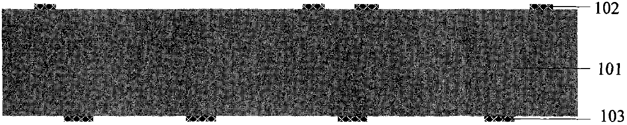
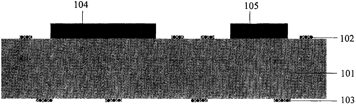
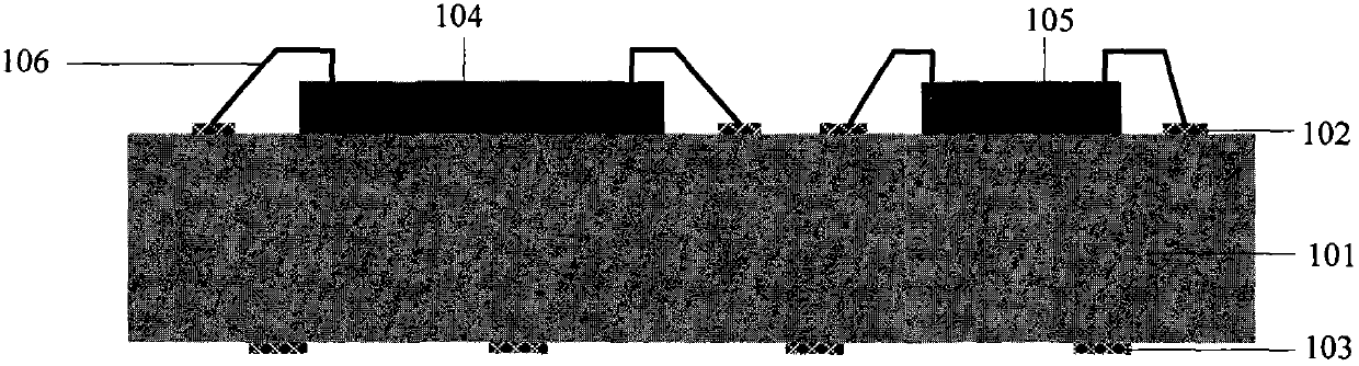
[0041] Figure 1a to Figure 1e It is a cross-sectional schematic diagram of a specific implementation process for completing an integrated satellite navigation chip according to the present invention.

[0042] Step 1, design and produce such as Figure 1a The shown two-layer printed circuit substrate 101 for realizing the logic connection and supporting function among multiple chips can be manufactured by conventional substrate technology, except that there are two layers on the substrate for realizing the functional electrical connection of the integrated navigation chip. The redistribution layer, and the pad structure 102 on the upper surface for the bonding wire pad of the surface die, generally composed of copper, nic...


PUM


Abstract

The invention discloses an integrated satellite navigation chip and a manufacture method thereof. The integrated chip comprises one or multiple substrates, bare chips, components, bonding wires and a BGA solder ball array, wherein the substrates are used for supporting functional chips to realize electrical connection between the functional chips, the bare chips and components of the radiofrequency, baseband, storage microprocessor and other functional chips are laid on the substrates in a stacked or planar manner, the bonding wires are used for realizing electrical connection among the functional chips as well as between the functional chips and the substrates, and the BGA solder ball array is formed at the back sides of the substrates via backflow in a C4 technology. The bare chips and components of the multiple functional chips for realizing Beidou&GPS dual-mode satellite navigation are integrated in a packaging body via a series of substrate and micro-assembly technologies to form a small electronic product with high performance, high density and low loss, reception and processing of Beidou&GPS dual-mode satellite navigation are realized, and the problems that a present satellite navigation product module is large in size, high in wring difficulty, high in cost and the like are solved.

Description

technical field [0001] The invention relates to the field of satellite navigation, in particular to a structure and a manufacturing method of a high-density and high-integration Beidou & GPS dual-mode satellite navigation integrated chip realized by using multi-chip packaging technology. Background technique [0002] The Beidou satellite navigation system is a global satellite navigation system with my country's independent intellectual property rights. With the gradual improvement of the construction of the Beidou satellite navigation system, the satellite navigation, precise timing and location service industries with Beidou as the core are playing an increasingly important role in the national economic life, becoming a crucial emerging industry, and the development prospects are very broad . [0003] High-performance satellite navigation terminals and chips are the core of satellite navigation systems and the foundation of the entire navigation service industry chain. A...

Claims


Application Information

Patent Timeline
IPC IPC(8): G01S19/13G01S19/35
CPCG01S19/35G01S19/33H01L25/50
Inventor 谢伟东潘小山
Owner BEIJING TIANZHONGLEI INTELLIGENT TECH
Features
  • Generate Ideas
  • Intellectual Property
  • Life Sciences
  • Materials
  • Tech Scout
  • Unparalleled Data Quality
  • Higher Quality Content
  • 60% Fewer Hallucinations
Learn More